JAJSBZ0D March 2014 – December 2017 UCC28630 , UCC28631 , UCC28632 , UCC28633 , UCC28634
PRODUCTION DATA.
- 1 特長
- 2 アプリケーション
- 3 概要
- 4 改訂履歴
- 5 Device Comparison Table
- 6 Pin Configuration and Functions
- 7 Specifications
-
8 Detailed Description
- 8.1 Overview
- 8.2 Functional Block Diagram
- 8.3
Feature Description
- 8.3.1 High-Voltage Current Source Start-Up Operation
- 8.3.2 AC Input UVLO / Brownout Protection
- 8.3.3 Active X-Capacitor Discharge (UCC28630 and UCC28633 only)
- 8.3.4 Magnetic Input and Output Voltage Sensing
- 8.3.5 Fixed-Point Magnetic Sense Sampling Error Sources
- 8.3.6 Magnetic Sense Resistor Network Calculations
- 8.3.7 Magnetic Sensing: Power Stage Design Constraints
- 8.3.8 Magnetic Sense Voltage Control Loop
- 8.3.9 Peak Current Mode Control
- 8.3.10 IPEAK Adjust vs. Line
- 8.3.11 Primary-Side Constant-Current Limit (CC Mode)
- 8.3.12 Primary-Side Overload Timer (UCC28630 only)
- 8.3.13 Overload Timer Adjustment (UCC28630 only)
- 8.3.14 CC-Mode IOUT(lim) Adjustment
- 8.3.15 Fault Protections
- 8.3.16 Pin-Fault Detection and Protection
- 8.3.17 Over-Temperature Protection
- 8.3.18 External Fault Input
- 8.3.19 External SD Pin Wake Input (except UCC28633)
- 8.3.20 External Wake Input at VSENSE Pin (UCC28633 Only)
- 8.3.21 Mode Control and Switching Frequency Modulation
- 8.3.22 Frequency Dither For EMI (except UCC28632)
- 8.4 Device Functional Modes
-
9 Applications and Implementation
- 9.1 Application Information
- 9.2
Typical Application
- 9.2.1 Notebook Adapter, 19.5 V, 65 W
- 9.2.2 UCC28630 Application Schematic
- 9.2.3 Design Requirements
- 9.2.4
Detailed Design Procedure
- 9.2.4.1 Custom Design With WEBENCH® Tools
- 9.2.4.2 Input Bulk Capacitance and Minimum Bulk Voltage
- 9.2.4.3 Transformer Turn Ratio
- 9.2.4.4 Transformer Magnetizing Inductance
- 9.2.4.5 Current Sense Resistor RCS
- 9.2.4.6 Transformer Constraint Verification
- 9.2.4.7 Transformer Selection and Design
- 9.2.4.8 Slope Compensation Verification
- 9.2.4.9 Power MOSFET and Output Rectifier Selection
- 9.2.4.10 Output Capacitor Selection
- 9.2.4.11 Calculation of CC Mode Limit Point
- 9.2.4.12 VDD Capacitor Selection
- 9.2.4.13 Magnetic Sense Resistor Network Selection
- 9.2.4.14 Output LED Pre-Load Resistor Calculation
- 9.2.5 External Wake Pulse Calculation at VSENSE Pin (UCC28633 Only)
- 9.2.6 Energy Star Average Efficiency and Standby Power
- 9.2.7 Application Performance Plots
- 9.3 Dos and Don'ts
- 10Power Supply Recommendations
- 11Layout
- 12デバイスおよびドキュメントのサポート
- 13メカニカル、パッケージ、および注文情報
9 Applications and Implementation
9.1 Application Information
The UCC2863x device is a highly integrated primary-side-regulated (PSR) flyback controller, supporting magnetically-sensed output voltage regulation via the transformer bias winding. This sensing eliminates the need for a secondary-side reference, error amplifier and opto-isolator for output voltage regulation. The device delivers accurate output voltage static load and line regulation, and accurate control of the output constant-current limit.
The fixed-point magnetic sampling scheme allows operation in both continuous conduction mode (CCM) and discontinuous conduction mode (DCM). The combination of the sampling scheme and high current gate driver source and sink capability, makes this device ideal for high power flyback converters up to 100 W and beyond.
The modulator adjusts both frequency and peak current in different load regions to maximize efficiency throughout the operating range. The control approach improves performance (efficiency, size and cost) and can reduce transformer size and cost by allowing operation in CCM with FM during peak overload conditions. The modulator supports peak-to-average transient overload power up to 200% of the nominal average rating.
9.2 Typical Application
9.2.1 Notebook Adapter, 19.5 V, 65 W
This design example describes the PWR572 EVM design and outlines the design steps required to design a constant-voltage, constant-current flyback converter for a 19.5-V/65-W notebook adapter. For all equations and design steps, refer to Table 7 for definitions and values of key internal device parameters that are relevant for calculations of external component values.
9.2.2 UCC28630 Application Schematic
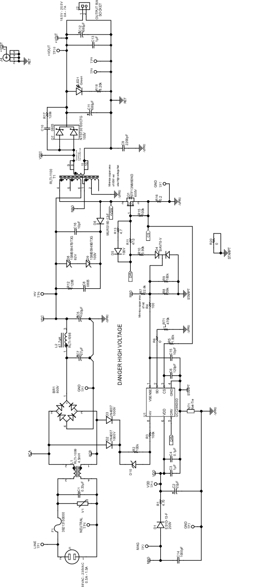 Figure 44. Typical Application Circuit for 19.5-V / 65-W Adapter
9.2.3 Design Requirements
Table 8. Design Requirements
| DESIGN PARAMETER | TARGET VALUE |
|---|---|
| Output voltage | 19.5 V |
| Rated (continuous) output power | 65 W |
| Peak (transient) output power | 130 W |
| Peak (transient) output power duration | 2 ms |
| Input AC voltage range | 88 VRMS to 264 VRMS |
| Typical efficiency | 88% |
| Minimum bulk voltage at 88 VAC/47 Hz and rated (continuous) output power | 82 V |
9.2.4 Detailed Design Procedure
9.2.4.1 Custom Design With WEBENCH® Tools
Click here to create a custom design using the UCC2863x device with the WEBENCH® Power Designer.
- Start by entering the input voltage (VIN), output voltage (VOUT), and output current (IOUT) requirements.
- Optimize the design for key parameters such as efficiency, footprint, and cost using the optimizer dial.
- Compare the generated design with other possible solutions from Texas Instruments.
The WEBENCH Power Designer provides a customized schematic along with a list of materials with real-time pricing and component availability.
In most cases, these actions are available:
- Run electrical simulations to see important waveforms and circuit performance
- Run thermal simulations to understand board thermal performance
- Export customized schematic and layout into popular CAD formats
- Print PDF reports for the design, and share the design with colleagues
Get more information about WEBENCH tools at www.ti.com/WEBENCH.
9.2.4.2 Input Bulk Capacitance and Minimum Bulk Voltage
The required bulk capacitance value depends on the target minimum bulk capacitor ripple voltage at minimum AC input line, minimum line frequency and on the power level of interest. As a way of estimating, use 1.5-μF to 2-μF per Watt of rated, continuous power to achieve approximately 70 V to 80 V minimum at 88 VRMS input. This case indicates a required bulk capacitance of between approximately 100 μF and 130 μF. Alternatively, the required capacitance may be explicitly calculated for a specific set of requirements using Equation 21.

Using the parameters in Table 8, this calculates a required CBULK of 130 μF.
To help reduce differential mode (DM) emissions for conducted EMC compliance, the bulk capacitance has been split into two separate capacitors C5 and C7 in Figure 44, with a small DM choke L2 inserted between the capacitors. The total resulting capacitance of 127 μF is close to the required minimum requirement per Equation 21, and the design results in a small decrease in the actual bulk capacitor minimum ripple voltage.
Next, verify that the choice of bulk capacitance satisfies the X-capacitor discharge constraints for rate of discharge by the load when X-capacitor sampling is inactive, per Equation 5. The bulk capacitance should be less than the value calculated by Equation 22.

9.2.4.3 Transformer Turn Ratio
Choose the transformer primary-to-secondary-side turns ratio based on the allowed voltage stress for the output rectifier, or the primary MOSFET. For 19.5-V charger designs, it is valid to choose a turns ratio that allows the use of a more efficient 100-V Schottky rectifier.

For a good Schottky diode with 100-V reverse rating, VREV(rated), the rectifier forward voltage drop, VRECT, can be expected to be in the range of 0.4 V to 0.5 V at 3 A to 5 A, at practical operating temperatures in the region of 100°C. Allowing an 85% derating on the rectifier reverse voltage stress, Equation 23 indicates a required turns ratio of 5.734 for a maximum AC peak voltage of 373 V (264 VRMS).
Choose the bias winding turns ratio to set the nominal bias voltage for the device VDD pin. Use an initial VBIAS(target) of 12 V.

where
- VF is the forward voltage drop of the rectifier on the bias winding.
For a typical 0.7-V bias-diode drop, this equation calculates to 0.6366.
When the transformer size and type are chosen, the actual turns values can be calculated. Because the turns need to be rounded to integer values, the actual turns ratios achieved deviates from these targets. Check the final ratios to ensure that the secondary-side Schottky rectifier stress and the bias winding nominal level are acceptable. Adjust the specific turns counts to meet the target ratios.
9.2.4.4 Transformer Magnetizing Inductance
Match the power stage design to the modulator curves by ensuring that the boundary conduction mode (BCM – boundary of operation between DCM and CCM) point coincides with the minimum bulk-capacitor voltage at minimum line, at rated output power. This choice results in DCM operation at all line voltages for all loads up to continuous rated load, and minimizes power loss and EMC impacts due to output rectifier reverse recovery during CCM operation. This design choice allows operation to extend into the CCM region of operation as required to deliver the transient peak load.
To achieve this design target, the required primary magnetizing inductance, LPRI is calculated from Equation 25. In this equation, the value of FSW(nom) is 60 kHz, taken from the modulator curve region P3 to P4, in Table 6. The value of VBULK(min) is the value that occurs with the actual used bulk capacitance of 127 μF.

This calculates a value of 257 μH. Round the value to 260 μH.
9.2.4.5 Current Sense Resistor RCS
In addition to choosing LPRI value to map the rated power to the target BCM point at minimum bulk voltage, choose the RCS value according to Equation 26. This calculation ensures that the resulting peak current, in conjunction with the chosen value of magnetizing inductance, and the 60-kHz modulator frequency, delivers the required input power to meet the rated output load power, at minimum bulk voltage ripple.

where
- VCS(bcm) is the modulator peak-current sense level at point P4 (640 mV)
This equation calculates a value of 207 mΩ. Use the nearest standard E24 value of 200 mΩ.
9.2.4.6 Transformer Constraint Verification
As outlined in Magnetic Sensing: Power Stage Design Constraints, there are constraints on the ratio of RCS/LPRI to ensure the design is consistent with the required volt-seconds for output sampling at minimum load, and with the controller tON(min) at high line. Per Equation 15 and Equation 16, limit the ratio of RCS/LPRI.

and,

In this case, the ratio equates to 769, so both constraints are met.
9.2.4.7 Transformer Selection and Design
After determining the value of current sense resistor RCS, determine the maximum peak current at maximum demand point on the modulator. Accommodate for the IPEAK adjustment for frequency dithering. Use this value when calculating the margin for core saturation. In this case, IPK(sat) calculates to 4.13 A.

In subsequent calculations of required primary turns etc, the average maximum peak current, IPK(max) , during the frequency dither period should be used, which calculates to 4.0 A.

Knowing IPK(max), LPRI and the turns ratio, the choice of transformer size and core shape and type dictates the required number of primary, secondary and bias turns, and the size of the air-gap. Various trade-offs, design preferences, and transformer design targets (size, cost, target losses, etc.) influence the specific choice of transformer core in any given design.
In the case of the UCC28630EVM-572 (PWR572 EVM), core area-product geometry was used to choose the minimum core size available to meet the power level. The core geometry factor Kg is a figure-of-merit that reflects the core power capability, in terms of its physical size, shape and design. It combines the core effective cross-sectional area, Ae, winding window area, Aw, and the mean length per turn (MLT) of wire around the core.

Estimate the required design core geometry, KG(des), using the required transformer inductance LPRI, maximum peak current IPK(max), allowed maximum core flux density Bmax and a target copper loss budget, PCU.

where
- ρcu is the resistivity of Copper (approximately 1.7 × 10⁻⁸ Ωm at room temperature, 2.2 × 10⁻⁸ Ωm at 100°C),
- Ku is a winding window utilization factor that accounts for the percentage of the window that is occupied by Copper
Ku can often be as low as 25%, due to the fill factor (gaps between wires), wire insulation (especially for triple-insulated wire), and the need for insulating tapes and EMC shielding layers. The estimate of the required core geometry needs an estimate of the aggregate total winding current ITOT. The analysis models the flyback transformer primary and secondary windings as a single lumped non-isolated inductor (such as a single winding buck inductor), only for the purpose of sizing the required core winding window to achieve the target copper loss. In this case, the secondary-side current amplitude reflects to the primary side so that aggregate total primary current. ITOT can be estimated in Equation 33.

where
- d is the primary on-time duty cycle
- dSEC is the secondary-side flyback period duty cycle
At rated power and minimum bulk capacitor voltage, the inductance LPRI has been chosen to achieve boundary-mode conduction, therefore the duty cycle is given in Equation 34.

and

At the boundary conduction point, the primary peak current IPK is at the level set by the modulator, VCS(bcm). So from Equation 33, ITOT becomes Equation 36.

Equation 36 calculates ITOT as 2.6 A. Thus the required design KG(des), assuming KU of 25%, Bmax of 315 mT and a target of 1-W copper loss, is shown in Equation 37.

Equation 37 indicates that this design requires a core size and shape with a KG of more than 6.9 × 10⁻¹². A review of commonly used cores indicated that the RM10/I core set meets this requirement. With Ae of 96.6 mm2, Aw of 44.2 mm2 and mean length per turn (MLT) of 52 mm, KG(RM10) is 7.9 × 10⁻¹², giving some margin over the design target.

With the chosen core, the actual primary, secondary-side and bias turns can be calculated. The required primary turns depend on the allowed Bmax. For most power ferrites, a value in the region of 315 mT is commonly used.

Round NP to 34. Now the required secondary-side turns can be calculated, using the previously calculated turns ratio per Equation 23.

Again, NS is rounded to 6. Due to the integer rounding of the turns count, ensure that the actual turns ratio is within 5% of original target (if outside this range, secondary-side rectifier or primary MOSFET stress may be too high).

From Equation 24, the required bias turns can be calculated using Equation 42.

Again, NB is rounded to 4. The effect of integer scaling in the turns is verified by calculating the expected bias voltage versus target.

The VBIAS target was 12 V, so this is acceptable.
The required core inductance factor, AL, to achieve the target inductance can be calculated as in Equation 44. The transformer manufacturer uses this factor to gap the core center leg.

Finally, calculate the required air-gap length lg, based on the required inductance and the core geometry.

where
- μ0 is the permittivity of free-air
- μr is the relative permeability of the chosen core ferrite material
- ACENTRE is the cross-sectional area of the core center leg
- lm is the core average magnetic path length
For the RM10/I core in 3C95 material (chosen for low core loss over a wide temperature range), the required air-gap length is calaulated using Equation 46.

Typically, the air-gap calculation in Equation 45 underestimates lg, due to flux fringing in the air-gap. The fringing causes the affective area of the air-gap Ag to be somewhat larger than the ferrite core center leg ACENTRE, depending on the gap length. This difference requires an increase in the required air-gap length to get the required inductance, which results in a further increase in fringing. However use Equation 45 to determine an initial value for lg, which can then be used to estimate Ag. For round centre legs, the increase in effective area within the gap can be estimated empirically from Equation 47

where
- DCENTRE is the center leg diameter
(For more information about this subject, download the paper Inductor and Flyback Transformer Design, Lloyd Dixon, TI Power Supply Design Seminar SLUP127).
Because Equation 45 assumes that Ag equals ACENTRE, it must be modified using Equation 48.

Re-iterating the air-gap calculation in Equation 49 .

Typically, after the second iteration above in Equation 48, the estimated air-gap is very close to the required value. Further iterations can be made, but should not be necessary.
9.2.4.8 Slope Compensation Verification
After choosing the current sense resistor, transformer inductance and transformer turns ratio, verify the required slope compensation against the fixed internal slope compensation. The worst case slope compensation requirement always occurs at the highest duty cycle operating point (at minimum bulk voltage level).
For stability, the slope compensation should be at least 50% of the difference between the inductor up-slope and down-slope. [reference Bob Mammano TI Power Supply Design Seminar paper, 2001, SLUP173]. For a flyback converter, the difference in slopes in CCM is equal the operating duty cycle multiplied by the inductor current down-slope value. For example, for 50% dBULK(min) at minimum bulk capacitor voltage, the required slope compensation ramp is 25% of the inductor current down-slope.
As listed in Table 8, the specified peak-load transient is 130 W for 2 ms. In a worst case, peak transient timing with respect to the AC phase, the VBULK minimum level dips to 65 V. This corresponds to a duty cycle of approximately 63.5% according to Equation 50.

The required slope compensation ramp is calculated at 63.5% duty cycle.

This value is within the 30 mV/μs of internal slope compensation provided by the controller.
9.2.4.9 Power MOSFET and Output Rectifier Selection
The initial design target proposed the use of a 100-V Schottky rectifier. The secondary-side reverse voltage stress can be verified using the final transformer design sh own in Equation 52.

The value derived from Equation 52 is close to the original design target of 85 V.
For 65-W load, the average DC output current is 3.35 A for 19.5-V output. However, to reduce losses, a much higher current rated diode is typically used, to yield a much lower forward voltage drop VRECT. As shown in Figure 44, a 30-A rated diode D7 is used in this case, with a forward drop of approximately 0.45 V at 3.5 A, 100°C.
For the primary-side MOSFET, the peak voltage stress can be estimated using Equation 53.

An allowance of at least 100 V must be added to this figure to account for the leakage inductance spike at turn-off. This voltage spike depends on the transformer implementation and the amount of leakage inductance, as well as the specific design of the snubber. A more aggressive snubber may reduce the voltage spike, but at the expense of higher losses in the snubber. A voltage rating of at least 600 V is recommended for the power MOSFET to allow for leakage.
The MOSFET rms current at low line, rated load, can be estimated using Equation 54.

As can be seen in Figure 44, the chosen MOSFET Q1 is a 13-A, 600-V device.
9.2.4.10 Output Capacitor Selection
Select the output capacitor value on the basis of one of the following, depending on which one is the limiting factor:
- Required ripple current rating to absorb the high secondary-side peak current
- Required esr to achieve a target peak-peak ripple voltage
- Required holdup capacitance to achieve target minimum output voltage for a specified load transient from no load when the device is switching at fSW(min)
For flyback converters, ripple current rating often dictates the output capacitance value. The required ripple current rating can be calculated from Equation 55.

At rated 65-W load, ICAP(rms) = 5.9 ARMS. Capacitors C11 and C13 in Figure 43 are chosen to meet this ripple requirement, (each capacitor has a 2.5-A minimum rating at 105°C). Total output capacitance is 1360 μF.
9.2.4.11 Calculation of CC Mode Limit Point
Calculate the expected output constant-current (CC) limit point from Equation 20. As previously noted, KCC1 is 44.5 and KCC1 is 69.5. Thus, IOUT(lim) in this case is approximately calculated in Equation 56.

9.2.4.12 VDD Capacitor Selection
Size the VDD capacitor to supply sufficient IDD(run) current to the device during initial start-up, and also during the charging phase of the main output capacitors. During the charging phase the bias winding on the transformer must supply the bias power. When VDD reaches the VDD(start) threshold, the device consumes IDD(run) for tSTART(del) before the PWM switching commences. Thereafter, the bias current is the device current plus the MOSFET gate current. The VDD capacitor must support this higher level of current until the output is sufficiently charged that the bias winding rail has increased above the VDD(stop) level.
Calculate the required bias capacitance from the total bias charge associated with the device run current during the tSTART(del) phase, plus the device run current during the output charge phase, plus the primary MOSFET gate charge current during the output charge phase. The time taken for the output charge phase to reach a sufficient level to supply the bias can be calculated from the size of the output capacitor, target output regulation voltage, and the difference between the available CC mode current limit and the maximum load current (assuming that the output capacitor has to be charged whilst also supplying full rated load current). Assume that the MOSFET is switched at 60 kHz throughout the charging phase.
Combining these into one equation, the required VDD capacitor can be calculated as shown in Equation 57.

This can be re-written with the explicit device values substituted:

For this EVM design, the MOSFET Qg(tot) is 30 nC, VBIAS(nom) is 12.6 V. IO(max) is 3.35 A, so this equates to:

Choose the next higher standard value, 22 μF.
Verify that the bias capacitance is sufficient to absorb all the X-capacitor energy when it has to be discharged, per Equation 3. From Figure 44, the value of X-capacitor is 330 nF.

9.2.4.13 Magnetic Sense Resistor Network Selection
The required values for the magnetic sense divider network are calculated from Equation 11 and Equation 12. For the RM10/I transformer used in the PWR572 EVM, the secondary-side to bias leakage inductance was measured and found to be approximately 4%. This figure can be reasonably estimated as the ratio of the inductance value measured across the secondary-side pins with the bias pins shorted together (primary winding should remain open-circuit), to the inductance value measured across the secondary-side pins with all other windings open:

RA is calculated as shown in Equation 62.

The nearest standard E96 value 22.6 kΩ is selected. RB may then be calculated to set VOUT at 19.5 V.

The nearest E96 value is 32.4 kΩ, which could be used, but results in some set-point regulation error. As shown in Figure 44, the setpoint may be fine-tuned by using two parallel resistors for RB. In this case use values of 39 kΩ and 180 kΩ, to give a net equivalent of 32.05 kΩ, very close to the target value in Equation 63.
Note that the pull-up diode to DRV pin should be a standard switching signal diode such as BAS21 or similar. The reverse recovery of the diode should be 100 ns or less. A slow-recovery diode clamps the VSENSE pin low for an initial portion of the flyback interval, and may impair or prevent the ability to take a valid output voltage sample.
9.2.4.14 Output LED Pre-Load Resistor Calculation
As shown in Figure 44, the output power good LED1 and series resistor R18 form an output pre-load or minimum load. This pre-load is necessary in order to maintain regulation at no load, or when the power converter output is disconnected from the load system. Magnetic regulation relies on sensing the output voltage during switching cycles, so it is necessary to maintain a certain minimum switching frequency fSW(min) in order to continue sensing the output voltage. However, generating switching cycles at fSW(min) transfers energy to the output, which requires some load on the secondary-side to absorb this energy and prevent the output capacitors from being charged out of regulation. The minimum energy transferred at fSW(min) depends on the choice of magnetizing inductance LPRI and current sense resistor RCS.

In order to ensure that the control loop operates at a frequency above the minimum switching frequency, fSW(min) (to ensure that the loop has adjustment range up/down as required to maintain regulation), the recommended minimum pre-load is at least twice the value calculated in Equation 64.
The required value of R18 can then be calculated, assuming a forward voltage drop of 1.8 V for the LED:

Use the next lower E24 value of 8.2 kΩ. For a design without an LED, a pre-load resistor of similar value is still required across the output voltage.
9.2.5 External Wake Pulse Calculation at VSENSE Pin (UCC28633 Only)
The typical application circuit of Figure 39 may be redrawn as a simplified equivalent circuit as shown in Figure 45. In this equivalent circuit, the capacitor CP is the total parasitic capacitance (MOSFET Coss, transformer capacitance, etc), and resistance RWAKE is the effective internal resistance of the UCC24650 WAKE pin to GND pin when the internal WAKE pull-down is active (see UCC24650 detailed datasheet specifications).
If all the elements on the primary and secondary of the transformer are referred to the bias winding, this can be further simplified as in Figure 46.
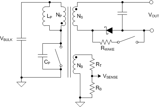 Figure 45. Simplified Equivalent Circuit of Wake Event with UCC24650
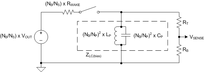 Figure 46. Bias-Referred Simplified Equivalent Circuit of Wake Event with UCC24650
Thus, knowing LP and CP, the power stage impedance ZLC(bias) (reflected to the bias winding) may be calculated from Equation 66, and the effective wake resistance can be referred to the bias winding using Equation 67. The wake pulse amplitude can be calculated from Equation 68. If CP is not known, it can be measured by observing the resonant ring period at the primary drain node, TRES, and calculating CP from Equation 69. Worst case values should be used to estimate the worst case minimum wake pulse amplitude at the VSENSE pin. It should also be noted that any filter cap on the VSENSE pin (including internal parasitic pin capacitance) adds an RC filter in conjunction with the Thevenin resistance of the VSENSE divider, RT, RB; this delays and further attenuate the wake pulse amplitude. Additionally, the internal wake comparator requires some over-drive to trip, and exhibits propagation delay that depends on the amount of overdrive. So some margin should be allowed in the wake pulse amplitude to ensure that the minimum wake pulse can adequately overdrive the internal wake comparator. A margin of at least 20% over the threshold VSENSE(wake) is recommended.


If the worst case wake pulse amplitude is too low, then the UCC24650 WAKE output can be augmented with an external PNP circuit Q1, R1 and R2, as shown in Figure 40. This circuit reduces the effective wake resistance to ground, so that a larger proportion of the output voltage appears across the transformer secondary pins when the UCC24650 WAKE activates.
Using the UCC28630EVM-572, (TI Literature Number SLUUAX9) circuit parameters from Figure 44, the nominal wake pulse amplitude at the VSENSE pin can be estimated. Of course, the rectifying diode D7 in Figure 44 would need to be relocated to return end of the secondary winding (pins 10, 11) to allow UCC24650 to be deployed.
From observation of the DCM ringing period, the period TRES was found to be 1.138 μs. From Equation 69, CP is estimated:

From Equation 66, the power circuit impedance is:

The WAKE pin resistance RWAKE can be determined form the UCC24650 datasheet; for now a nominal value of 400 Ω is assumed. Referred to the bias winding (scaled by (NB/NS)2), this becomes 178 Ω. Similarly ΔWAKE% can be determined from the UCC24650 datasheet; for now, a value of 97% is assumed. From Equation 68, the wake pulse amplitude can be calculated:
In this case, the VSENSE wake pulse amplitude would be insufficient to trip the internal wake comparator. If the power stage had higher LP, or lower CP, a larger wake pulse would be produced.
Alternatively, the effective wake resistance RWAKE may be reduced by adding the PNP circuit per Figure 40. This has been verified using Q1 = FMMTA92 PNP transistor, R1= 100 Ω and R2 = 2.2 kΩ. A wake pulse amplitude of almost 2 VPK was produced at the VSENSE pin, giving generous margin to the internal threshold VSENSE(wake). The observed waveforms are shown in Figure 47 for a worst case 0% to 100% (65 W) load transient (where the PWM is at FMIN). The PWM is re-activated when VOUT has dropped by ~3%, rather waiting for the next timed wake-up (~5 ms later).
Figure 48 shows a zoomed waveform of the wake pulsing ringing as measured on the bias winding. It can be seen that the peak level is approximately 3 VPK, which would produce a pulse of approximately 1.8 V at the VSENSE pin (scaled by VSENSE divider resistors RT and RB). As noted in Test and Debug Recommendations, the VSENSE pin should never be directly probed, doing so affects the regulation setpoint.
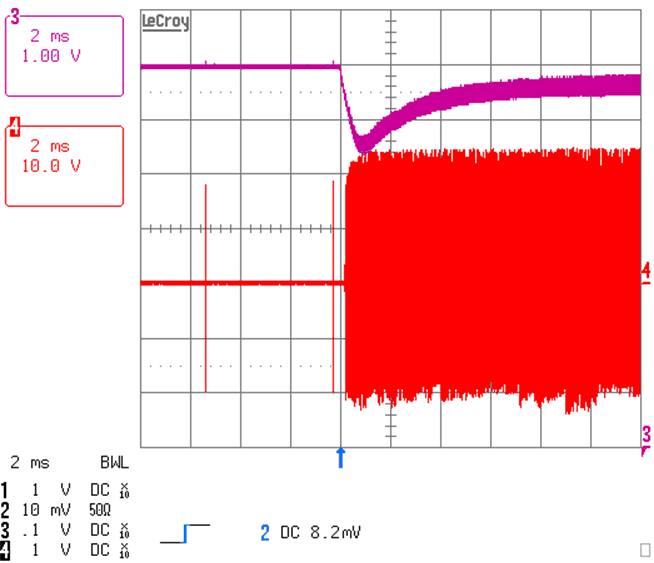 Figure 47. Observed Output Voltage (Ch3) and Bias Winding (Ch4)
 (showing wake event generated by UCC24650)
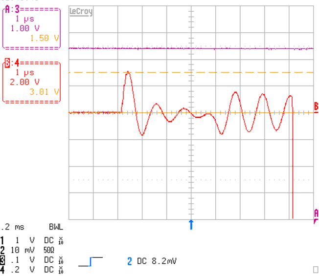 Figure 48. Zoom In of Wake-Pulse Ringing
 (observed across bias winding (ChB) generated by UCC24650)
9.2.6 Energy Star Average Efficiency and Standby Power
Table 9 summarize the standby power, and Table 10 summarizes the average efficiency performance of the UCC28630EVM-572, (TI Literature Number SLUUAX9).
Table 9. Standby Power Performance
| STANDBY POWER | |
|---|---|
| 115 VAC (mW) | 230 VAC (mW) |
| 57 | 60 |
Table 10. Average Efficiency Performance
| AVERAGE EFFICIENCY (INCLUDING OUTPUT 76-mΩ CABLE DROP) | ||
|---|---|---|
| LOAD LEVEL (%) | 115 VAC (%) | 230 VAC (%) |
| 25 (16.25 W) | 89.44 | 89.26 |
| 50 (32.5 W) | 88.98 | 89.38 |
| 75 (48.75 W) | 88.24 | 89.10 |
| 100 (65 W) | 87.59 | 88.73 |
| Average | 88.6 | 89.1 |
9.2.7 Application Performance Plots
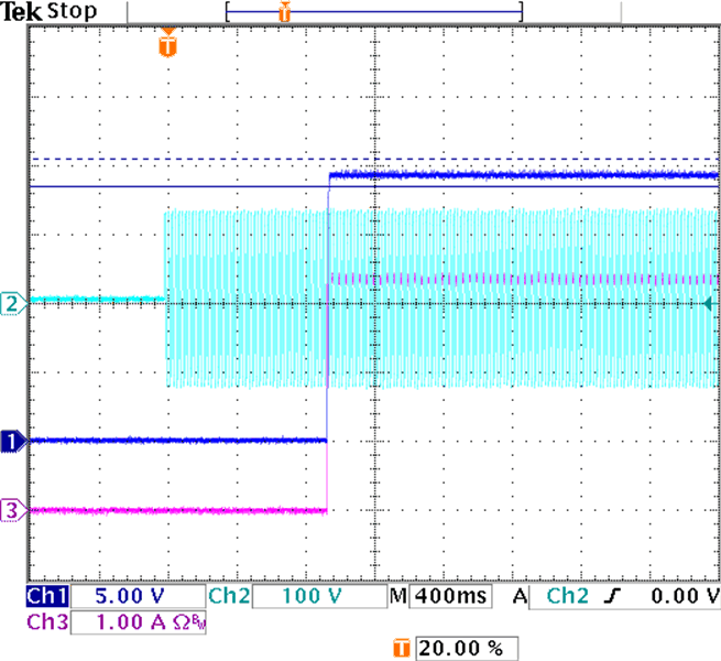 Figure 49. Start-Up from 90-VAC, 3.35-A CC Load
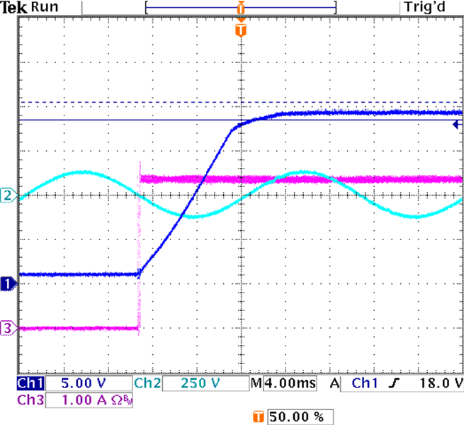 Figure 51. Output Rise-Time, 90-VAC, 3.35-A CC Load
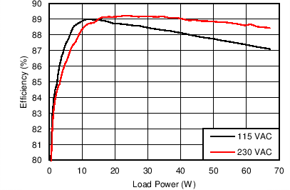 Figure 53. Efficiency vs. Load/Line
 (cable drop included)
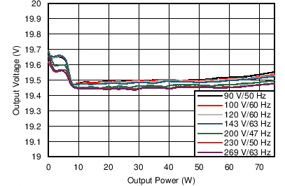 Figure 55. Output Voltage Regulation vs. Line/Load
 (without cable drop)
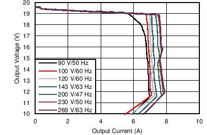 Figure 57. CC Mode Regulation vs. Line
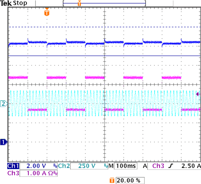 Figure 59. Transient Step 50% to 100% Load, 115 VAC
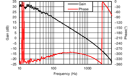 Figure 61. Measured Control Loop Gain/Phase at 300 VDC, Full Load 3.35 A
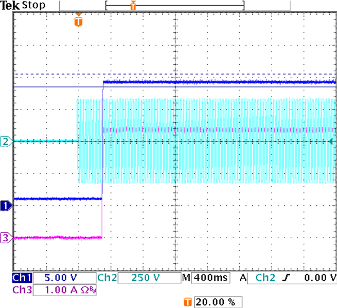 Figure 50. Start-Up from 230-VAC, 3.35-A CC Load
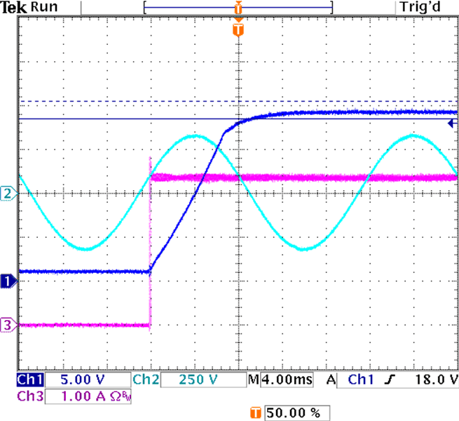 Figure 52. Output Rise-Time, 230-VAC, 3.35 A CC Load
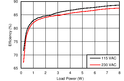 Figure 54. Zoom Light-Load Efficiency vs. Load/Line
 (cable drop included)
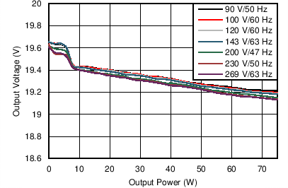 Figure 56. Output Voltage Regulation vs. Line/Load
 (with cable drop included)
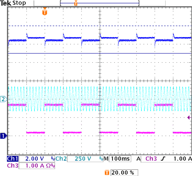 Figure 58. Transient Step 5% to 50% Load, 115 VAC
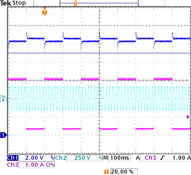 Figure 60. Transient Step 10% to 90% Load, 115 VAC
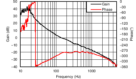 Figure 62. Measured Control Loop Gain/Phase at 300 VDC, Light Load 0.2 A
9.3 Dos and Don'ts
9.3.1 Test and Debug Recommendations
One important precaution must be noted during test and debug. Do not probe the VSENSE pin with an oscilloscope probe, meter or differential probe. Doing so adds excessive capacitance to the pin, delaying the pin rise-time, and causing the regulated system output voltage to increase.
