JAJSBZ0D March 2014 – December 2017 UCC28630 , UCC28631 , UCC28632 , UCC28633 , UCC28634
PRODUCTION DATA.
- 1 特長
- 2 アプリケーション
- 3 概要
- 4 改訂履歴
- 5 Device Comparison Table
- 6 Pin Configuration and Functions
- 7 Specifications
-
8 Detailed Description
- 8.1 Overview
- 8.2 Functional Block Diagram
- 8.3
Feature Description
- 8.3.1 High-Voltage Current Source Start-Up Operation
- 8.3.2 AC Input UVLO / Brownout Protection
- 8.3.3 Active X-Capacitor Discharge (UCC28630 and UCC28633 only)
- 8.3.4 Magnetic Input and Output Voltage Sensing
- 8.3.5 Fixed-Point Magnetic Sense Sampling Error Sources
- 8.3.6 Magnetic Sense Resistor Network Calculations
- 8.3.7 Magnetic Sensing: Power Stage Design Constraints
- 8.3.8 Magnetic Sense Voltage Control Loop
- 8.3.9 Peak Current Mode Control
- 8.3.10 IPEAK Adjust vs. Line
- 8.3.11 Primary-Side Constant-Current Limit (CC Mode)
- 8.3.12 Primary-Side Overload Timer (UCC28630 only)
- 8.3.13 Overload Timer Adjustment (UCC28630 only)
- 8.3.14 CC-Mode IOUT(lim) Adjustment
- 8.3.15 Fault Protections
- 8.3.16 Pin-Fault Detection and Protection
- 8.3.17 Over-Temperature Protection
- 8.3.18 External Fault Input
- 8.3.19 External SD Pin Wake Input (except UCC28633)
- 8.3.20 External Wake Input at VSENSE Pin (UCC28633 Only)
- 8.3.21 Mode Control and Switching Frequency Modulation
- 8.3.22 Frequency Dither For EMI (except UCC28632)
- 8.4 Device Functional Modes
-
9 Applications and Implementation
- 9.1 Application Information
- 9.2
Typical Application
- 9.2.1 Notebook Adapter, 19.5 V, 65 W
- 9.2.2 UCC28630 Application Schematic
- 9.2.3 Design Requirements
- 9.2.4
Detailed Design Procedure
- 9.2.4.1 Custom Design With WEBENCH® Tools
- 9.2.4.2 Input Bulk Capacitance and Minimum Bulk Voltage
- 9.2.4.3 Transformer Turn Ratio
- 9.2.4.4 Transformer Magnetizing Inductance
- 9.2.4.5 Current Sense Resistor RCS
- 9.2.4.6 Transformer Constraint Verification
- 9.2.4.7 Transformer Selection and Design
- 9.2.4.8 Slope Compensation Verification
- 9.2.4.9 Power MOSFET and Output Rectifier Selection
- 9.2.4.10 Output Capacitor Selection
- 9.2.4.11 Calculation of CC Mode Limit Point
- 9.2.4.12 VDD Capacitor Selection
- 9.2.4.13 Magnetic Sense Resistor Network Selection
- 9.2.4.14 Output LED Pre-Load Resistor Calculation
- 9.2.5 External Wake Pulse Calculation at VSENSE Pin (UCC28633 Only)
- 9.2.6 Energy Star Average Efficiency and Standby Power
- 9.2.7 Application Performance Plots
- 9.3 Dos and Don'ts
- 10Power Supply Recommendations
- 11Layout
- 12デバイスおよびドキュメントのサポート
- 13メカニカル、パッケージ、および注文情報
7 Specifications
7.1 Absolute Maximum Ratings(1)
over operating junction temperature range (unless otherwise noted)| MIN | MAX | UNIT | ||
|---|---|---|---|---|
| Start-up pin voltage | HV | 700 | V | |
| Bias supply voltage | VDD | 20 | ||
| Current sense input voltage | CS | –0.3 | 1.5 | |
| All other input pins | VSENSE | –0.3 | VDD | |
| SD | –0.3 | VDD | ||
| Operating junction temperature range, TJ | –40 | 125 | °C | |
| Storage temperature, Tstg | -65 | 125 | ||
| Lead temperature | 260 | |||
(1) Stresses beyond those listed under absolute maximum ratings may cause permanent damage to the device. Exposure to absolute-maximum-rated conditions for extended periods may affect device reliability. These are stress ratings only and functional operation of the device at these or any other conditions beyond those indicated under recommended operating conditions is not implied. All voltages are with respect to GND. These ratings apply over the junction operating temperature ranges unless otherwise noted.
7.2 ESD Ratings
| VALUE | UNIT | |||
|---|---|---|---|---|
| V(ESD) | Electrostatic discharge(3) | Human-body model (HBM), per ANSI/ESDA/JEDEC JS-001(1) | ±2000 | V |
| Charged-device model (CDM), per JEDEC specification JESD22-C101(2) | ±500 | |||
(1) JEDEC document JEP155 states that 500-V HBM allows safe manufacturing with a standard ESD control process. Manufacturing with less than 500-V HBM is possible with the necessary precautions. Pins listed as ±2000 V may actually have higher performance.
(2) JEDEC document JEP157 states that 250-V CDM allows safe manufacturing with a standard ESD control process. Manufacturing with less than 250-V CDM is possible with the necessary precautions. Pins listed as ±500 V may actually have higher performance.
(3) Electrostatic discharge (ESD) to measure device sensitivity and immunity to damage caused by assembly line electrostatic discharges into the device.
7.3 Recommended Operating Conditions
over operating junction temperature range (unless otherwise noted)| MIN | NOM | MAX | UNIT | ||
|---|---|---|---|---|---|
| CS input | 0 | 1.0 | V | ||
| All other inputs (except HV, CS) | 0 | VDD | |||
| SD pin external capacitance | 0 | 1 | nF | ||
| RHV, external resistor on HV pin, see Figure 15 | 180 | 200 | 220 | kΩ | |
| RP, external pull-up resistor on VSENSE pin, see Figure 21 | 3.8 | 3.9 | 4.0 | ||
7.4 Thermal Information
| THERMAL METRIC(1) | UCC28630 | UCC28631 | UNIT | |
|---|---|---|---|---|
| D | D | |||
| 7 PINS | 7 PINS | |||
| θJA | Junction-to-ambient thermal resistance | 128.5 | 128.5 | °C/W |
| θJCtop | Junction-to-case (top) thermal resistance | 57.3 | 57.3 | |
| θJB | Junction-to-board thermal resistance | 83.4 | 83.4 | |
| ψJT | Junction-to-top characterization parameter | 12.3 | 12.3 | |
| ψJB | Junction-to-board characterization parameter | 82.1 | 82.1 | |
| THERMAL METRIC(1) | UCC28632 | UCC28633 | UCC28634 | UNIT | |
|---|---|---|---|---|---|
| D | D | D | |||
| 7 PINS | 7 PINS | 7 PINS | |||
| θJA | Junction-to-ambient thermal resistance | 128.5 | 128.5 | 128.5 | °C/W |
| θJCtop | Junction-to-case (top) thermal resistance | 57.3 | 57.3 | 57.3 | |
| θJB | Junction-to-board thermal resistance | 83.4 | 83.4 | 83.4 | |
| ψJT | Junction-to-top characterization parameter | 12.3 | 12.3 | 12.3 | |
| ψJB | Junction-to-board characterization parameter | 82.1 | 82.1 | 82.1 | |
(1) For more information about traditional and new thermal metrics, see the IC Package Thermal Metrics application report, SPRA953.
7.5 Electrical Characteristics
over operating junction temperature range (unless otherwise noted) and VDD = 12 V| PARAMETER | TEST CONDITIONS | MIN | TYP | MAX | UNIT | |
|---|---|---|---|---|---|---|
| START-UP CURRENT SOURCE | ||||||
| IVDD0 | VDD pin short-circuit charging current | VDD = 0.2 V, VHV = 100 V | 0.6 | 0.9 | 1.2 | mA |
| IVDD1 | VDD pin final charging current | VDD = 11.9 V, VHV = 100 V | 1.1 | 4.0 | 7.6 | mA |
| ILEAK | HV current source leakage current | VDD = 18 V, VHV = 100 V HV, current source off, TA = 25°C |
0.1 | 0.5 | μA | |
| SUPPLY VOLTAGE MONITORING | ||||||
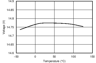
| VDD(start) | VDD start-up voltage | VDD increasing | 13.00 | 14.75 | 16.50 | V |
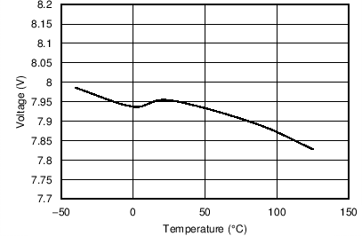
| VDD(stop) | VDD minimum operating voltage after start-up | VDD decreasing after start-up | 7.3 | 8.0 | 8.5 | V |
| VDD(hyst) | VDD start – VDD stop level | 6.5 | V | |||
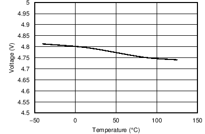
| VDD(reset) | VDD reset restart level | 3.5 | 5.0 | 6.5 | V | |
| VDD(ovp) | VDD over-voltage protection level | VDD increasing after start-up, UCC28630, UCC28631, UCC28632, UCC28633 | 16.5 | 17.5 | 18.3 | V |
| VDD increasing after start-up, UCC28634 only | 14.0 | 14.85 | 15.55 | V | ||
| IDD(run) | Supply current during normal operation | VSENSE = 0.45 V, CS = 0 V See (1) CLOAD = 700 pF on DRV | 6.0 | 9.0 | 13.0 | mA |
| IDD(sleep) | Supply current during sleep mode, between switching pulses | VSENSE = 8.0 V, VCS = 1.0 V, light-load mode at 200 Hz, TA = 25°C | 90 | 110 | μA | |
| OSCILLATOR | ||||||
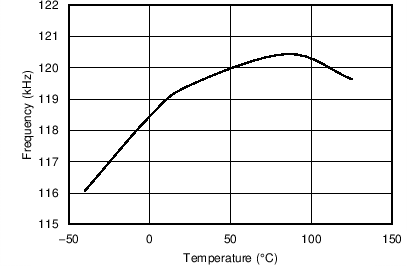
| fSW(max) | Maximum switching frequency | VSENSE = 0.45 V, VCS = 0 V | 110 | 120 | 130 | kHz |
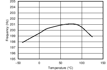
| fSW(min) | Minimum switching frequency | VSENSE = 8.0 V, VCS = 1.0 V, light-load mode | 0.18 | 0.20 | 0.22 | kHz |
| DMAX | Maximum Duty Cycle | VSENSE = 0.45 V, VCS = 0 V | 70% | |||
| tON(min) | Minimum On time | VSENSE = 8.0 V, VCS = 1.0 V, light-load mode | 550 | 600 | 650 | ns |
| fSW(dith) | Frequency dither range | Except UCC28632 | ± 6.7% | |||
| tDITH | Dither repetition period | Except UCC28632 | 6.0 | ms | ||
| SHUTDOWN (SD) PIN (EXTERNAL FAULT INPUT)(2) | ||||||
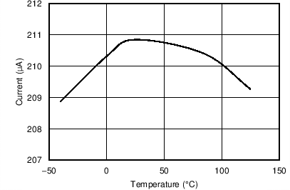
| IPULLUP | Internal pull-up current source | See (2), (3), (4) | 185 | 210 | 235 | µA |
| VTRIP(rise) | Fault ok level (rising) | See (2), (3), (4) , UCC28630, UCC28631, UCC28632,UCC28633 | 3.2 | 3.5 | 3.8 | V |
| See (2), (3), (4) , UCC28634 only | 2.2 | 2.5 | 2.8 | V | ||
| VTRIP(fall) | Fault trip level (falling) | See (2), (3), (4) | 1.7 | 2.00 | 2.3 | V |
| VTRIP(hyst) | See (2), (3), (4) | 1.5 | V | |||
| VWAKE(rise) | Wake-up level (rising) | See (2), (3), (4)Except UCC28633 | 1.8 | 2.2 | 2.6 | V |
| tWAKE | Wake delay time | Delay to first DRV pulse | 10 | µs | ||
| VSENSE Pin (MAGNETIC SENSE) | ||||||
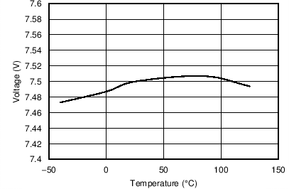
| VOUT(ref) | Internal output voltage sense reference level | Required positive voltage at VSENSE pin during off-time (at 25°C) | 7.425 | 7.500 | 7.575 | V |
| tOUT(smp) | Vsense sample delay for VOUT | Measured w.r.t. DRV falling edge | 1.7 | µs | ||
| VOUT(ovp) | Internal output voltage sense OVP level | Measured w.r.t. regulation level, tracking | 120% | |||
| CURRENT SENSE (CS) Pin | ||||||
| VCS(max) | Peak CS pin voltage level | At maximum modulator demand | 800 | mV | ||
| VCS(min) | Peak CS pin voltage level | At minimum modulator demand | 172 | mV | ||
| VSLOPE | Slope compensation ramp | 30 | mV/µs | |||
| OVER TEMPERATURE PROTECTION | ||||||
| TEMPTRIP | Thermal protection shutdown temperature | Default internal setting, latch-off protection | 125 | °C | ||
| TEMPHYST | Thermal protection hysteresis | 10 | °C | |||
| GATE DRIVE OUTPUT (DRV) | ||||||
| ROH | High level source resistance | IOH = 100 mA | 22 | 35 | Ω | |
| ROL | Low level sink resistance | IOL = –100 mA | 1.2 | 2.5 | Ω | |
(1) CLOAD = 700 pF included on DRV pin.
(2) The SD pin functions as an NTC input pin (with internal pull-up) during normal operation. The internal pull-up is clamped to 4 V. At start-up, the external temperature sensor (NTC) must be cool enough that the SD pin pulls up above the VTRIP(rise) start level. After start-up, if this pin is pulled below VTRIP(fall) level, this activates external over-temperature shut-down.
(3) During low power modes (when FSW < FSMP(max)), the internal SD pin pull-up is disabled, and the pin functions as a transient wake-up input. In this case, if the pin is raised above VWAKE(rise) level, the device wakes from low power sleep mode (rather than waiting for the scheduled timer-based wake). This is useful for applications that require a response to load transients from zero or near-zero load, where a wake-up signal can be appropriately coupled to the SD pin from the secondary-side.
(4) A decoupling capacitor on the SD pin should not be required; if used, it must not exceed 1 nF.
7.6 Typical Characteristics
A.
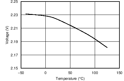
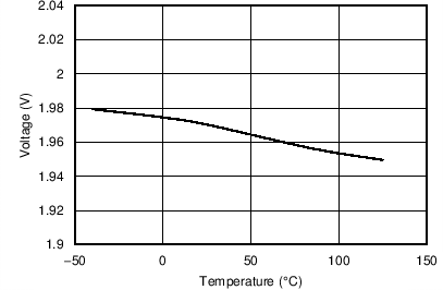
Figure 7. VDD(reset) Threshold vs. Temperature
A.
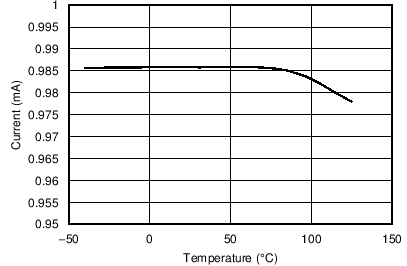
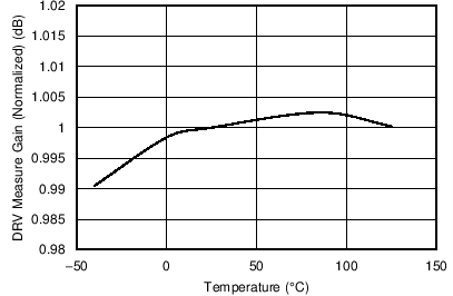
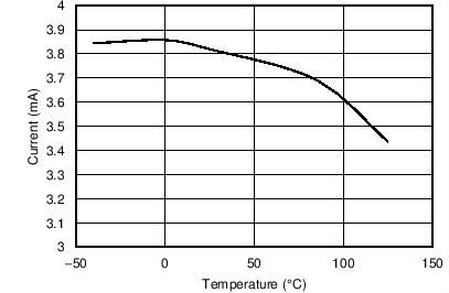
Figure 2. IVDD1 Charging Current vs. Temperature
