JAJSBZ0D March 2014 – December 2017 UCC28630 , UCC28631 , UCC28632 , UCC28633 , UCC28634
PRODUCTION DATA.
- 1 特長
- 2 アプリケーション
- 3 概要
- 4 改訂履歴
- 5 Device Comparison Table
- 6 Pin Configuration and Functions
- 7 Specifications
-
8 Detailed Description
- 8.1 Overview
- 8.2 Functional Block Diagram
- 8.3
Feature Description
- 8.3.1 High-Voltage Current Source Start-Up Operation
- 8.3.2 AC Input UVLO / Brownout Protection
- 8.3.3 Active X-Capacitor Discharge (UCC28630 and UCC28633 only)
- 8.3.4 Magnetic Input and Output Voltage Sensing
- 8.3.5 Fixed-Point Magnetic Sense Sampling Error Sources
- 8.3.6 Magnetic Sense Resistor Network Calculations
- 8.3.7 Magnetic Sensing: Power Stage Design Constraints
- 8.3.8 Magnetic Sense Voltage Control Loop
- 8.3.9 Peak Current Mode Control
- 8.3.10 IPEAK Adjust vs. Line
- 8.3.11 Primary-Side Constant-Current Limit (CC Mode)
- 8.3.12 Primary-Side Overload Timer (UCC28630 only)
- 8.3.13 Overload Timer Adjustment (UCC28630 only)
- 8.3.14 CC-Mode IOUT(lim) Adjustment
- 8.3.15 Fault Protections
- 8.3.16 Pin-Fault Detection and Protection
- 8.3.17 Over-Temperature Protection
- 8.3.18 External Fault Input
- 8.3.19 External SD Pin Wake Input (except UCC28633)
- 8.3.20 External Wake Input at VSENSE Pin (UCC28633 Only)
- 8.3.21 Mode Control and Switching Frequency Modulation
- 8.3.22 Frequency Dither For EMI (except UCC28632)
- 8.4 Device Functional Modes
-
9 Applications and Implementation
- 9.1 Application Information
- 9.2
Typical Application
- 9.2.1 Notebook Adapter, 19.5 V, 65 W
- 9.2.2 UCC28630 Application Schematic
- 9.2.3 Design Requirements
- 9.2.4
Detailed Design Procedure
- 9.2.4.1 Custom Design With WEBENCH® Tools
- 9.2.4.2 Input Bulk Capacitance and Minimum Bulk Voltage
- 9.2.4.3 Transformer Turn Ratio
- 9.2.4.4 Transformer Magnetizing Inductance
- 9.2.4.5 Current Sense Resistor RCS
- 9.2.4.6 Transformer Constraint Verification
- 9.2.4.7 Transformer Selection and Design
- 9.2.4.8 Slope Compensation Verification
- 9.2.4.9 Power MOSFET and Output Rectifier Selection
- 9.2.4.10 Output Capacitor Selection
- 9.2.4.11 Calculation of CC Mode Limit Point
- 9.2.4.12 VDD Capacitor Selection
- 9.2.4.13 Magnetic Sense Resistor Network Selection
- 9.2.4.14 Output LED Pre-Load Resistor Calculation
- 9.2.5 External Wake Pulse Calculation at VSENSE Pin (UCC28633 Only)
- 9.2.6 Energy Star Average Efficiency and Standby Power
- 9.2.7 Application Performance Plots
- 9.3 Dos and Don'ts
- 10Power Supply Recommendations
- 11Layout
- 12デバイスおよびドキュメントのサポート
- 13メカニカル、パッケージ、および注文情報
8 Detailed Description
8.1 Overview
The UCC28630, UCC28631, UCC28633, UCC28633 and UCC28634 family of devices are highly-integrated, primary-side-regulated (PSR) flyback controllers. The device supports magnetically-sensed output voltage regulation via the transformer bias winding. This feature eliminates the need for a secondary-side reference, error amplifier and opto-isolator. The device employs an advanced internal control algorithm that offers accurate static output voltage regulation against line and load. The fixed-point, magnetic-sampling scheme allows operation in both continuous conduction mode (CCM) and discontinuous conduction mode (DCM). Additionally, the device achieves accurate constant-current (CC) control of the output current limit using only primary-side, current sensing. Uniquely, this CC function operates seamlessly as the operating mode changes between DCM and CCM operation.
The controller includes an internal, high-voltage (HV) start-up current-source, and employs low-power sleep modes and switching frequency reduction, to improve light-load efficiency and standby power. The device typically achieves standby power levels between 0.05% and 0.1% of peak output power.
The controller operates in either DCM and CCM, using a mix of peak current-mode PWM (AM) and switching-frequency modulation (FM) schemes. The control approach improves performance (efficiency, size and cost) and can reduce transformer size and cost by allowing operation in CCM with FM during peak overload conditions. Extensive protection features are incorporated, including output overvoltage protection (OVP), bias rail overvoltage and undervoltage (OV/UV), active X-capacitor discharge, line undervoltage and brownout protection, overcurrent overload timer, open- and short-circuit pin protections, peak current adjustment with line and frequency dither for system EMI reduction. The various devices in the UCC2863x family offer a different mix of features to suit a wide range of applications and requirements.
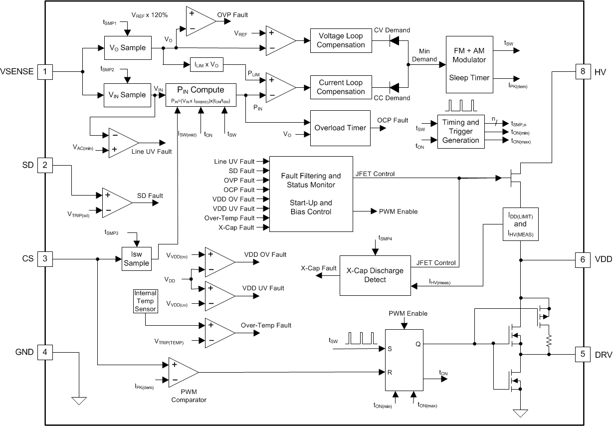
8.2 Functional Block Diagram
8.3 Feature Description
The application designer requires some key device internal parameters in order to calculate the required power stage components and values for a given design specification. Table 7 summarizes the key parameters.
8.3.1 High-Voltage Current Source Start-Up Operation
The controller includes a switched, high-voltage, current source on the HV pin to allow fast start-up, and eliminates the static power dissipation in a conventional resistive start-up approach. This feature reduces standby power consumption.
The HV pin has three major functions:
- Supply the device start-up current
- Supply the device bias power during latched fault mode
- AC sense input for X-capacitor discharge detect (UCC28630 and UCC28633 only)
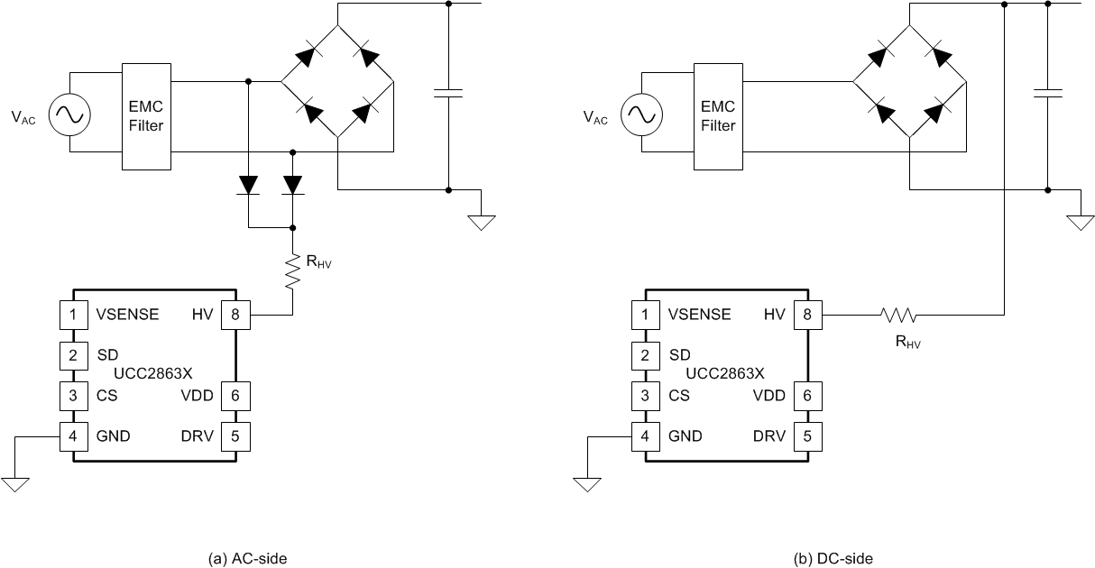
The UCC28630 and UCC28633 input supply to the HV start-up pin must be connected to the AC side of the bridge rectifier as shown in Figure 15, in order to support X-capacitor discharge. More details are given in Active X-Capacitor Discharge (UCC28630 and UCC28633 only), below. Connection to the AC side of the bridge also allows faster detection of AC mains removal under latched fault conditions, allowing prompt reset of latched faults for fast restart.
In the UCC28631, UCC28632 and UCC28634, the HV pin can connect to either the AC or DC side of the bridge. The addition of the 200-kΩ external HV resistance (required for X-capacitor discharge sensing) limits the available charging current for the external bias supply input capacitor. However, for typical values of between 22 µF and 33 µF of input capacitance, start-up bias times of less than 1.5 s are achievable at 90 VAC. Start-up time can be estimated using Equation 1.
For 90 VAC, if CVDD = 22 µF and worst case VDD(start_max) = 16.5 V, then tSTART is 1.002 s.
Figure 16 illustrates the start-up behavior of the controller. The HV current source has built-in short-circuit protection that limits the initial charge current out of the bias voltage pin until the bias voltage reaches VDD(sc). This limits the power dissipated in the HV current source in the event of a short circuit on the VDD pin. Thereafter, the HV current source switches to full available current. The controller remains in a low-power, start-up mode until the bias voltage reaches VDD(start), after which the HV current source is turned off and the controller initiates a start-up sequence.
The bias voltage decays during the start-up sequence at a rate dependent on the size of the energy storage capacitor connected to the VDD pin. The VDD storage capacitor must be sized appropriately to ensure adequate energy storage to supply both the controller bias power and MOSFET drive power during start-up, until the VDD rail can be supplied through the transformer bias winding. If the bias voltage falls below VDD(stop) (due to bias winding fault or an inadequate VDD storage capacitance), the controller stops switching, and transitions into low-power mode for a time delay of tRESET(long), or until the bias voltage falls to the VDD(reset) level, whichever is shorter. See VDD Capacitor Selection for required VDD capacitor sizing. Once the time delay elapses, the bias voltage rapidly discharges to the VDD(reset) level, followed by turn-on of the internal HV current source, and a normal restart attempt follows.
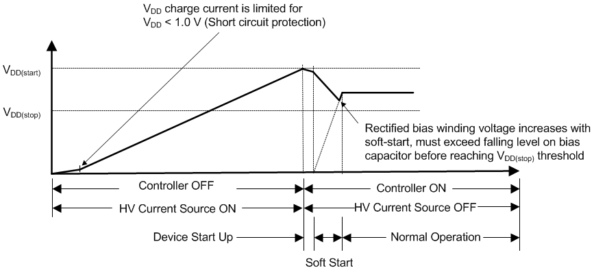 Figure 16. Normal Start-Up Sequence,
 (assuming VAC > UV start threshold)
8.3.2 AC Input UVLO / Brownout Protection
At start-up, once the VDD pin has reached the VDD(start) level, the internal start-up current source is turned off. The controller tests the voltage across the bulk capacitor to determine if the level is high enough to allow the power stage to start, if it has exceeded the rising ACON level. Because there is no load across the bulk capacitor at this stage, the bulk voltage can be used as a proxy for the peak of the AC line. In order to measure the bulk voltage in a low-loss fashion, the controller generates a sequence of three exploratory switching pulses at a frequency of fSW(uv), at minimum peak-current demand level VCS(min) to avoid audible noise, and to deliver minimum energy to the output of the power stage.
Based on the magnetic sampling information determined via the bias winding during these switching pulses, if the output voltage is greater than the output overvoltage threshold, the pulsing stops immediately, and the controller transitions into latched-fault mode. If, however, there is no overvoltage condition detected at the output, the pulse-set completes. If the sensed line voltage is above the line ACON start threshold, then the controller starts up normally, and begins to generate the PWM drive pulses that charge and regulate the output voltage. Alternatively, if the sensed bulk level is below the ACON threshold, then the controller enters low power mode for the reset period (tRESET(short)). It then depletes the VDD rail to the VDD(reset) level. At this point, the start-up sequence repeats, and the device generates another set of exploratory switching pulses. This sequence repeats indefinitely until the AC input is increased to a sufficient level that the bulk voltage exceeds the ACON level.
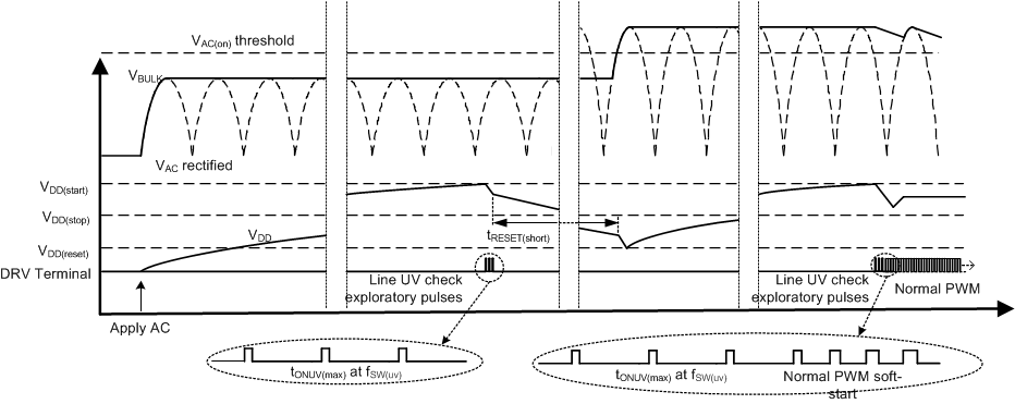 Figure 17. AC Input UVLO Detection and Start Up
Once started, the controller regularly monitors the bulk capacitor voltage. Because the ripple on the bulk capacitor depends on the load level, the device determines the maximum bulk level every 11 ms (approprite for minimum AC frequency of 47 Hz), so the AC peak can be determined. The controller provides input undervoltage protection based on the sensed AC peak level. Once the peak drops below the ACOFF level for the delay period (tUV(delay)), the PWM switching halts, and the controller enters low-power mode for the reset period (tRESET(short)). The device then discharges the bias voltage to the VDD(reset) level, followed by a restart sequence. The controller cycles through the ACON, monitoring (detailed above) indefinitely until the AC input again rises above the ACON level.
8.3.3 Active X-Capacitor Discharge (UCC28630 and UCC28633 only)
Safety standards such as EN60950 require that any X-capacitors in EMC filters on the AC side of the bridge rectifier quickly discharge to a safe level when AC is disconnected. This discharge requirement ensures that any high-voltage level present at the pins of the AC plug does not present an electric shock hazard. The standards require that the voltage across the X-capacitor decay with a maximum time constant of 1 second. Typically, this requirement is achieved by including a resistive discharge element in parallel with the X-capacitor. However, this resistance causes a continuous power dissipation that impacts the standby power performance. The power dissipation in the discharge resistors depends on the X-capacitor value. Assuming that the discharge resistor meets the 1-second time-constant requirement, (in other words, the R-C product is 1 second) the dissipation is described in Equation 2.

Thus at 230 VAC, the discharge resistor causes 5.3-mW dissipation for every 100 nF of X-capacitance – for a typical 470-nF X-capacitor value, that causes 25 mW to be lost in the discharge resistors.
The safety standard does not mandate that the X-capacitor is fully discharged to zero within one second. It simply requires the discharge rate to exhibit a 1-s time constant. Figure 18 shows the discharge characteristic (for a 1-s discharge time constant) versus time, for disconnection at the peak of 90 VAC, 115 VAC, 230 VAC and 264 VAC. For AC inputs above 115 VAC, with 1-s discharge time constant, the voltage does not drop below the Safety-Extra-Low-Voltage (SELV) 60-V level until 1 s or longer. In fact, at 264 VAC, 1.83 seconds elapse before reaching 60 V.
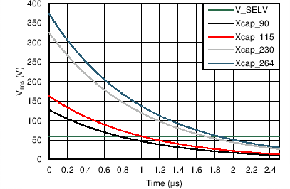 Figure 18. X-Capacitor Discharge with 1-s Time Constant, for Various Voltages
8.3.3.1 Improved Performance with UCC28630 and UCC28633
In order to reduce standby power and eliminate the standing loss associated with the conventional discharge resistors, the UCC28630 and the UCC28633 devices incorporate active X-capacitor discharge circuitry. This circuit periodically monitors the voltage across the X-capacitor to detect any possible DC-condition (which would indicate that AC mains disconnection has occurred), and then discharges the voltage across the X-capacitor using the internal HV current source. The X-capacitor discharge function discharges the X-capacitor to the SELV 60-V level in 1 s (as long as the design considerations discussed in this section are followed).
The device internally monitors the current into the HV pin to determine if the voltage across the X-capacitor in the EMI filter has a sufficient AC ripple component. If insufficient AC content is detected, then a DC condition is internally flagged. This causes the controller to enter low-power mode for the reset period (tRESET(short)), followed by bias voltage discharge to the reset level (VDD(reset)) , and then the start-up HV current source turns on again to effectively discharge the X-capacitor by transferring charge to the VDD reservoir capacitor.
Because the device monitors the HV pin to detect a DC condition on the X-capacitor, the system cannot operate with DC input to the HV pin. Instead, the HV pin must be connected to an AC source only. The device interprets any DC input on the HV pin as DC across the X-capacitor, indicating an AC-disconnect event. This causes a repeating cycle of start-up and shutdown. The device requires an external 200-kΩ of resistance on the HV pin, to limit the current to a level below the saturation point of the internal HV current source. This limit produces a HV input current that is approximately proportional to AC line, so that the AC content can be sensed.
The size of the X-capacitor that can be discharged depends on the VDD energy storage capacitor. Assuming the worst case, a maximum X-capacitor disconnect voltage could be at the peak of 264 VRMS, and assuming that it should be discharged down to 60-V SELV level, the minimum allowed VDD capacitor can be sized based on the worst case VDD(reset) and VDD(start) levels as described in Equation 3.

For example, for a 330-nF X-capacitor value, the required VDD capacitor is 15.9 µF, so a 22-µF capacitor suffices.

In order to reduce the power consumption from the high voltage AC line, the device pulses current into the HV pin at a low frequency with very low duty-cycle. The HV current source on-time (tON(HV)) , repeats at intervals of tSMP(HV). Moreover, the pulsing occurs in bursts, with a time delay between bursts. The sampling occurs in bursts of 21, at intervals of tSMP(HV), with a wait time of tWAIT(HV) between bursts. This reduces the effective average duty-cycle to a very low value (approximately 0.2%), and minimizes the overhead of X-capacitor sampling current and device bias consumption overhead to approximately 2 mW of extra standby consumption at high-line 230 VAC.
The device enables the X-capacitor monitor in latched fault mode, and in light-load regions where the power level is below PLL(%), as a percentage of the nominal rated level. Above the PLL(%) level, the X-capacitor monitor is disabled. At this load level the bulk capacitor discharges at a rate that is sufficient to also discharge the X-capacitor, which appears in parallel with the bulk capacitor once the bulk voltage drops far enough to forward bias the bridge rectifier diodes. In this case ensure that the bulk capacitance value is not too large for the power level desired, which in-turn ensures that the bulk capacitor discharge rate is fast enough to discharge the X-capacitor to meet the 1-s discharge target. This can be calculated in Equation 5.

Assuming a worst case AC disconnect at the peak at 264 VRMS (373 VPK), and a requirement to discharge to SELV level of 60 V in tXCAP(dis) of 1 s, for a PNOM of 65 W at 87% efficiency, this is calculated in Equation 6.

Once the bulk capacitance value is chosen, also ensure that when the bulk capacitor has been discharged down to the line UV ACOFF threshold, that it continues to discharge to an acceptable level during the line UV persistence delay time (tUV(delay)) as shown in Equation 7.
Again, taking the example above:

Once the first constraint is satisfied, the second one is also automatically met.
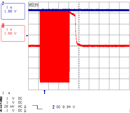 Figure 19. X-Capacitor Discharge Activation, at 230 VAC, No Load
 (red = X-capacitor, blue = bulk-capacitor, both 100 V/div)
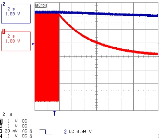 Figure 20. X-Capacitor Decay Rate Without Active Discharge
 (time constant dominated by 20-MΩ probe impedance)
(red = X-capacitor, blue = bulk-capacitor, both 100 V/div)
8.3.4 Magnetic Input and Output Voltage Sensing
A sense winding on the transformer is used to measure the input voltage and output voltage of the power stage. This winding is typically the converter bias winding. The sense winding should be interfaced to the VSENSE pin as shown in Figure 21. This interface requires that the voltage across the winding be scaled with a resistor divider RA / RB, and then offset with a switched, pull-up resistor RP (in series with a diode) connected to the gate drive pin DRV.
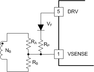 Figure 21. VSENSE Pin Interface Arrangement
During the off-time portion of the switching cycle (also referred to as the flyback interval), the resistor divider (RB / (RA + RB)) scales the positive voltage swing at the VSENSE pin for output voltage regulation, as shown in Figure 22. During this interval, since the DRV output is low, the diode in series with RP is reverse-biased, and so RP is out-of-circuit.
 Figure 22. VOUT Sense Using the Positive Swing on the Sense Winding
During the on-time portion of the switching cycle, when the DRV pin goes high (should swing very close to the value at the VDD pin), the switched pull-up RP allows the negative swing on the winding to be level-shifted positive, and thus also be sensed at the VSENSE pin, as shown in Figure 23. In this way the bias winding may be used to sense both line input voltage and output voltage.
NOTE
The input voltage sensed by the transformer bias winding is actually the voltage across the bulk capacitor, not the AC input voltage, because the bulk capacitor voltage appears across the primary winding when the flyback switch turns on
Uses of the sensed bulk and output voltages:
- Input AC mains UVLO
- Input brownout
- Line-dependent peak-current adjustment
- Accurate output-current regulation
- Output-voltage regulation
- Output over-voltage protection (OVP)
 Figure 23. Line Input Sense by Offsetting the Negative Swing on the Sense Winding
In order to protect the VSENSE pin from excessive negative current in the event of a manufacturing fault (such as an open circuit on RP), use a series limiting resistor and clamping diode on the VSENSE pin. Combine the clamping diode and DRV pull-up diode into a single-package common-cathode diode to reduce the component count of the system. This is illustrated in Figure 24.
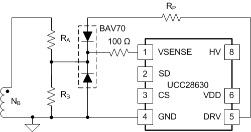 Figure 24. VSENSE Pin Protection and Interface to Bias Winding
The device continually adjusts the input voltage sample delay, measuring the sample half-way through the on-time interval, to ensure the cleanest signal. The device uses same mid-point sample trigger when measuring the main MOSFET switch current (ISW). Sampling MOSFET switch current in the middle of the on-time automatically measures the average current during the on-time, ISW(on_avg), which is required for the current limit and overload timer block.
The output voltage sample point is always time relative to the turn-off instant. Internally, the device uses the CS pin to determine the cycle end, rather than the PWM falling edge on the DRV pin. The device bases this determination on the instant that the MOSFET switch current drops below the demanded peak current level (IPEAK ) at the peak current mode comparator. Some delay always occurs from the falling edge on DRV to the point when the external power MOSFET turns off. This internal timing method ensures a more accurate measure of ISW(on_avg), and also ensures that the output voltage sample point is not measured too early, before the leakage ringing has subsided. The effect of the gate turn-off delay and the adjustment of the output voltage sample point is illustrated in Figure 25.
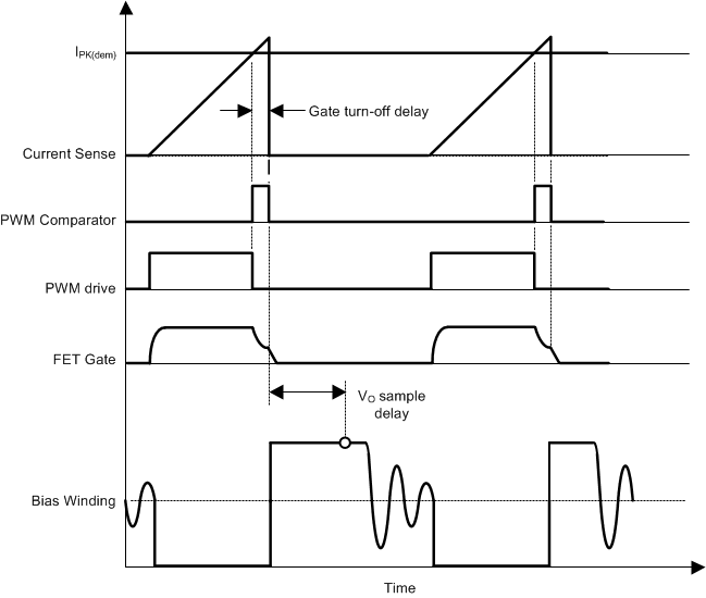 Figure 25. VOUT Sample Adjust for External Gate Delay
The sampling of the input voltage and output voltage signals on the bias winding must be synchronized to the on-time and off-time flyback intervals respectively, because the signals occur during only those intervals in the switching cycle. Typical waveforms and timing are illustrated in Figure 26.
More conventional knee-point detection schemes, where the sample is measured at the end of the flyback interval when the secondary-side current has decayed to zero, inherently always operate in discontinuous conduction mode (DCM). However, the fixed sample-point scheme used on the UCC2863x has the advantages of being able to operate in regions of fixed frequency, and being able to operate in continuous conduction mode (CCM). Fixed sample-point schemes conventionally suffer poorer regulation than knee-point schemes, because there is always current flowing at the sample instant. This current produces a sensing error as a result of the voltage drop produced across the secondary-side resistance and leakage inductance. This parasitic voltage drop varies with output voltage, line and load, thus influencing the regulation. The UCC2863x devices uses a novel internal compensation scheme to adjust for this parasitic voltage drop, and can deliver excellent static line and load regulation, even when operating heavily in CCM.
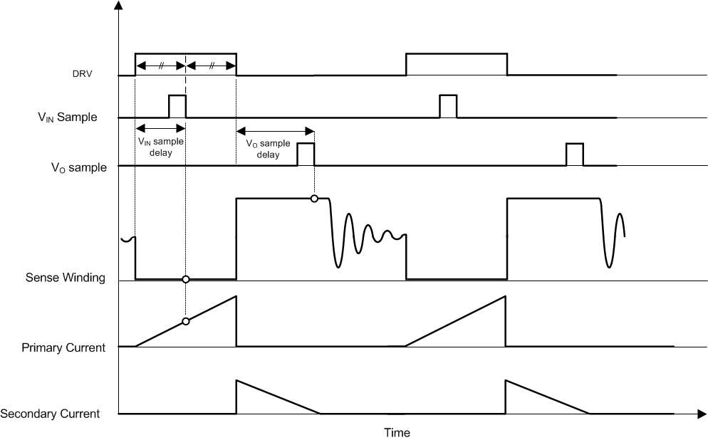 Figure 26. VIN and VOUT Sample Trigger Timing
8.3.5 Fixed-Point Magnetic Sense Sampling Error Sources
To support operation in CCM, and allow operation at fixed frequency over a large percentage of the load range, the UCC2863x uses fixed-point sampling rather than knee-point detection. When conventionally used, fixed-point sampling typically suffers from poorer regulation performance. This poor performance results from the voltage drops across the secondary-side parasitic resistance RSEC, and the secondary-side leakage inductance from secondary-side to bias LLK(sec_bias), as a consequence of the fact that current remains flowing on the secondary-side when the device measures the output voltage. As shown in Figure 27, the secondary-side pin voltage that gets reflected to the bias winding is detailed in Equation 9.

Equation 9 can be expanded and rearranged into Equation 10.

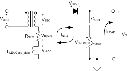 Figure 27. Secondary-Side Pin Voltage Contributors with Secondary-Side Current Flow
Many elements contribute errors to the sensed secondary-side pin voltage, when measured across the bias winding:
- VL(leak): Negative voltage drop across the sec-bias leakage inductance LLK(sec_bias); assuming constant regulated output voltage, this voltage drop is fixed constant offset, because VOUT/LSEC is constant as long as the output is in regulation.
- VRECT: Positive voltage drop across the output rectifier (assuming use of a conventional diode). This voltage drop varies with load current and temperature. However, a constant nominal voltage drop can usually be used, because the increasing forward voltage drop with increasing load current is largely cancelled by the decrease in forward drop as a result of the temperature rise that results.
- VR(sec): This is the drop across the secondary-side winding resistance. This value depends on loading, and varies in proportion to the primary peak current demand that is set by the modulator.
- VRC(esr): This is the drop across the output capacitor equivalent series resistance (esr). This value depends on the difference between the secondary-side winding current and the DC load current being drawn.
Typically, the peak secondary-side winding current ISEC is many times larger than the load current, and the secondary-side winding resistance is typically larger than the output capacitor esr. Thus, the last term in Equation 10 involving ILOAD can typically be neglected.
The leakage inductance and secondary-side rectifier terms represent quasi-constant offset terms, so do not affect regulation to a significant extent. Thus, the quasi-constant offset terms can be accounted for in the calculation of the required scaling resistors to produce the desired setpoint voltage.
The remaining term that dominates the regulation error in Equation 10 is the drop across the secondary-side winding resistance and capacitor esr at the sample instant, {ISEC x(RSEC + RC(esr))}. The controller internally adjusts the control loop reference in proportion to the primary peak current demand in order to null the ISEC related error term in the sampled bias winding voltage. Since the peak secondary-side current ISEC(pk) is the primary peak current IPRI(pk) scaled by the transformer turns ratio, the internal control loop reference effectively varies in approximate proportion to ISEC, resulting in dramatically improved regulation performance.
This improved regulation performance allows the use of primary-side regulation in a wider range of applications, and at unprecedented power levels, operating in both CCM and DCM.
8.3.6 Magnetic Sense Resistor Network Calculations
Because the device uses the VSENSE pin to measure both VOUT and VIN of the power stage, it is important to calculate the resistor values correctly. The step-by-step design process is outlined in this section.
8.3.6.1 Step 1
Depending on the power level, choice of transformer size, and required trade-offs between primary MOSFET and secondary-side rectifier ratings, the transformer turns NP, NS and NB will be chosen first. The controller can support a wide range of turns ratios.
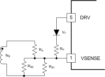 Figure 28. Practical Magnetic Sense Setup with Extra Resistor RB2 for Setpoint Fine Adjust
8.3.6.2 Step 2
Once NP, and NB are known, the required value of RA in Figure 28 is calculated using Equation 11.

In this equation, the internal controller gain KLINE is 49.25 (see Table 7 for key internal controller parameters), and the internal gains are designed for a fixed value for RP, (i.e. RP MUST be 3.9 kΩ).
8.3.6.3 Step 3
Once NS, target VOUT, output rectifier drop VRECT, and the secondary-side-to-bias leakage inductance LLK(sec_bias) are known, the required value for RB can be calculated. Referring to Equation 10, LLK(sec_bias) can be approximated as a percentage of the secondary-side-referred magnetizing inductance LSEC. (See Magnetic Sense Resistor Network Selection for details).

In this case, RB may need to be empirically adjusted to achieve the required exact output set-point, especially if VRECT varies or is not known precisely. For this reason, it is recommended that RB should be implemented on the system PCB as two parallel resistors RB1 and RB2 as shown in Figure 28, to allow easier fine-tuning of set-point. For set-point tuning, only RB should be adjusted. RA should never be adjusted, because to do so would affect the line sense gain and introduce errors into the line voltage measurement.
8.3.6.4 Step 4
Verify that the equivalent Thevenin resistance RTH of the RA/RB combination falls in the required range of 10 kΩ to 20 kΩ.


If the Thevenin resistance is outside of that range, then the original choice of turns ratio must be adjusted, and design steps repeated until a valid value for RTH is determined. This is unlikely to occur in practice, unless an extreme turns ratio is chosen. If RTH is outside this range, it triggers the VSENSE pin open or short pin-check at start-up.
8.3.7 Magnetic Sensing: Power Stage Design Constraints
Because the controller employs fixed-point sampling for output voltage sensing, there are some transformer design constraints that must be observed. The minimum magnetizing volt-seconds during the on-time interval occurs at the minimum CS pin voltage, VCS(min), under light-load conditions. This minimum should be the case at all line voltages, because the controller compensates for line-dependent peak-current overshoot during turn-off delay. The choice of transformer turns ratio, transformer inductance (LPRI), and current sense resistance (RCS) must ensure that the corresponding reset volt-seconds during the flyback interval are sufficient that a valid output sample is available at the sample point, tOUT(smp). This constraint is summarized in Equation 15.

where
- VRECT is the voltage drop across the output rectifier
Additionally, the device requires a minimum on-time, tON(min) , to ensure enough time for the system input voltage (VIN) and switch current (ISW ) to be measured. To meet the minimum on-time requirement at maximum line, and minimum load, the ratio of current sense resistance (RCS) to transformer inductance (LPRI) must meet the constraint shown in Equation 16.

Equation 15 or Equation 16 sets the limit for the ratio of RCS to LPRI, but both need to be verified. See Typical Application for more details.
8.3.8 Magnetic Sense Voltage Control Loop
Because the output voltage feedback is inherently a sampled signal obtained from the bias winding, the internal voltage control loop is most naturally implemented digitally. The internal control loop implements the equivalent of a PID loop in digital form. Because the output can be sampled only at certain intervals in each switching cycle, the sample rate is naturally tied to the switching frequency, and the sample rate increases with increasing frequency. However, the device clamps the sample rate at a normalized maximum rate, fSMP(max). But because the device must always synchronize to the next available switching cycle to obtain a new sample of the output voltage, the effective sample rate varies somewhat around this value.
The digital control loop compensator block diagram is shown in Figure 29. A new sample of output voltage is supplied to the compensator at the normalized maximum clock rate (fSMP(max)) , or fSW, whichever is lower. An updated output voltage demand signal, yk, is produced at the same clock rate. This voltage loop demand represents the required operating point on the modulator curves to keep the output voltage in regulation. The modulator sets the appropriate switching frequency and peak current demand depending on the load power.
 Figure 29. Digital Voltage Control Loop Simplified Block Diagram
The control loop PID gain factors are internally fixed values, optimized for flyback power stages in the range between 20 W and 130 W. The loop is designed to work with magnetizing inductance values in the range between 200 µH and 1500 µH. Assuming that the output capacitance value is chosen based on required ripple current rating, then loop stability is not a problem. Adding extra output capacitance does not degrade the loop performance and the resulting extra output hold-up improves transient response.
The Typical Application section includes gain-phase measurements taken using the 65-W UCC28630EVM-572 evaluation module.
8.3.9 Peak Current Mode Control
The controller operates in peak current mode. The primary-side switch (MOSFET) current is sensed by a shunt resistor (RCS1) connected in series with the source of the FET as shown in Figure 30. The voltage that is developed across the sense resistor is connected to the CS pin of the controller. The device uses the current sense signal at the CS pin to terminate the PWM pulse according to the peak current demand of the modulator. The device automatically applies slope compensation as soon as the duty cycle of the DRV pin pulse exceeds 50%. This compensation provides stable operation up to maximum DRV duty cycle. The device applies this slope compensation as a downslope on the demand signal at the PWM comparator, so is not measureable at the CS pin. The device synchronizes the slope compensation signal to the PWM and is active only between 50% and 70% duty cycle, as shown in Figure 31.
Normal operating range for the CS pin is between 0 mV and 800 mV. The RCS1 resistor should be scaled such that the peak current at maximum peak load and minimum bulk capacitor voltage produces a signal of approximately 800 mV peak at the CS pin. This resistor value is calculated in conjunction with the calculation of the required primary magnetizing inductance, as outlined in Notebook Adapter, 19.5 V, 65 W, section.
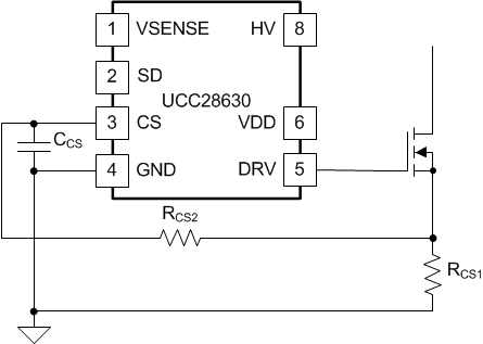 Figure 30. Primary-Side Current Sensing
A nominal 100 ns of filtering that is internal to the CS pin helps filter the leading turn-on spike of current. Depending on PCB layout, an RC filter (RCS2 and CCS) may be required on the CS pin as shown in Figure 30 to filter noise and spikes. The capacitor CCS should be positioned as close as possible to pins 3 and 4 and tracked directly to the pins. Series resistor RCS2 should also be located close to pin 3 to minimize noise pick-up. RCS2 value should not exceed 20 kΩ, because a larger value could be detected as a possible open circuit on the CS pin during the start-up pin-fault checks. The R-C filter time constant should not be excessive (timing between 100 ns and 200 ns is typical). Otherwise the filter reduces the measured peak current, and allows greater actual peak current to flow versus the modulator demand level. Such effects force the regulation loop to reduce the switching frequency to compensate, and at highest line, no load, this can lead to regulation difficulties if the control loop attempts to drop the frequency so far that it reaches the fMIN limit.
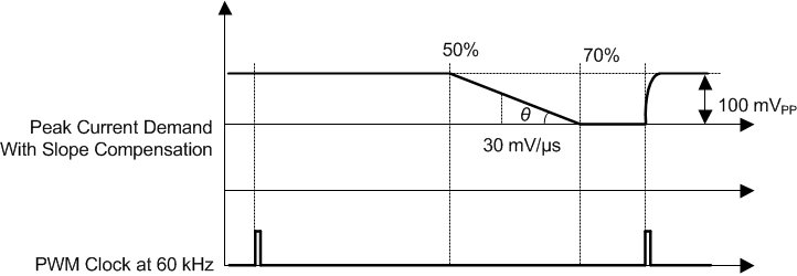 Figure 31. Peak Current Demand with Slope Compensating Downslope
8.3.10 IPEAK Adjust vs. Line
The controller applies a line-dependent reduction in the peak-current demand to correct for the current overshoot due to the PWM and gate drive propagation delay, with the aim of delivering a constant peak current versus line at a given power level. This maintains approximately constant switching frequency versus line for a given power level (until the operation enters into CCM), improves regulation, reduces audio noise, and allows lower standby power at high line. If not corrected, the current overshoot could become significant at high line, where the inductor current di/dt is higher. This overshoot would cause a pronounced increase in transferred power per switching cycle at high line, because power is proportional to IPK2. The effect of the delay on the peak-current overshoot is illustrated in Figure 32.
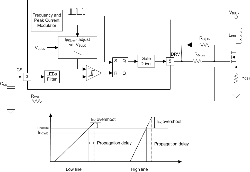 Figure 32. Peak-Current Demand Adjustment vs VBULK to Correct Prop Delay Overshoot
For different power stage designs, the combination of primary magnetizing inductance LPRI, current sense resistance RCS and external MOSFET gate turn-off delay tOFF(ext), must be verified against Equation 17, to ensure that the internal peak-current compensation gain range is satisfied. The KLINE(adj) factor should be within the range indicated. If the external turn-off delay is too long, then the internal IPEAK adjustment factor is too low, and the adjustment at high line is not able to achieve the required level of over-shoot compensation. As noted previously, this could result in regulation difficulties at no-load, and may cause poor line and load regulation, or require an increase in output pre-load power.

where
- where tPROP(gate) is the internal controller gate-drive turn-off propagation delay, given in Table 7.
8.3.11 Primary-Side Constant-Current Limit (CC Mode)
In addition to the peak-current mode PWM function, the device also uses sensed current at the CS pin to estimate the secondary-side load current. The device samples the CS pin voltage and measures it in the middle of the on-time, which is effectively the average switch current during the on time, ISW(avg_on). This measurement scheme is the case during both DCM and CCM operational modes. The average switch current during the on time is scaled by the PWM duty cycle to give the IIN(avg) of the power stage. The power stage input power, PIN, can then be estimated as the product of (VIN x IIN(avg)). The CC mode operation regulates PIN to track (IOUT(lim) x VOUT), if PIN increases to reach PIN(lim), thereby achieving a regulated constant current as shown in Equation 18.


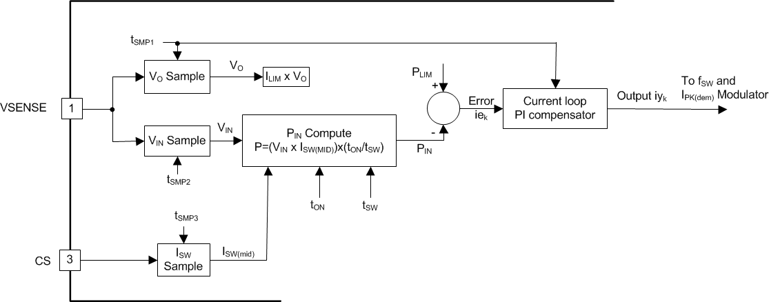 Figure 33. Digital Current Control Loop Simplified Block Diagram
Assuming that the power stage efficiency does not change significantly with operating point, by regulating the input power in inverse proportion to output voltage, this regulates output current. This achieves a brick-wall CC characteristic, where the output current is regulated as the input voltage changes and as the output voltage rolls off, regardless of power stage operating mode (CCM or DCM). The CC mode protection eliminates the characteristic load current tail-out that is typically seen with peak-current mode control as output voltage collapses and operation goes deeper into CCM mode.
NOTE
As the output voltage decreases in CC mode, the VDD level also decreases. If the overload is severe, the drop in output voltage causes VDD to drop below the VDD(stop) UV level. This drop causes a shutdown for tRESET(long), as given in Table 7, followed by a restart attempt.
The constant-current mode output current limit level (IOUT(lim)) is a function of both the RCS1 resistor and the transformer turns ratio. The device uses an internal reference and gain for the CC loop, KCC1 and KCC2, that set the CC IOUT(lim) point as a function of the chosen turns ratio, output voltage and current sense resistance as shown in Equation 20.

For the UCC28631, UCC28632 and the UCC28633 devices, the IOUT(lim) can be adjusted to be a percentage of the maximum value calculated by equation Equation 20. see CC-Mode IOUT(lim) Adjustment for more details.
8.3.12 Primary-Side Overload Timer (UCC28630 only)
The internal overload timer in the UCC28630 uses the same output load current measurement that is used by the CC loop. This measurement tracks the power stage thermal stress, and protects the power stage against output overload. If the output is overloaded for too long such that the power stage would be over-stressed, then the PWM shuts down, and enters low-power mode for a time period of tRESET(long); thereafter the device discharges VDD to the VDD(reset) level and initiates a hiccup mode restart.
The overload timer operates by taking an estimate of output current, squaring it (assuming the power stage losses are dominated by resistive I2 losses) to produce (K x I2OUT), where K is a scaling gain factor. The overload timer is constantly running at every load level, and accumulates at a rate dependent on the difference between (K x I2OUT) and the previous level of the timer. If (K x I2OUT) is greater than the previous timer level, the timer level continues to increase; if (K x I2OUT) is less than the previous timer level, then the timer level decreases. At any steady load, the overload timer level eventually settles at a level proportional to I2OUT. Because the overload timer level adjusts at a rate dependent on the difference between (K xI2OUT) and the previous level, the timer initially reacts faster to larger differences, but over time settles exponentially at a level proportional to (K x I2OUT).
As shown in Figure 34, in both the first and second examples, the initial steady load allows the timer to integrate and settle at a level proportional to the load. The margin to the over-load trip level depends on the historical loading, lower prior average loading results in greater future over-load capability, and vice versa. The rate at which the timer reacts to different load steps is set by the chosen time constant (or response rate) per Table 2.
The overload timer can cope with pulsed loads and loads with a complex waveform. Because the rate of increase and decrease also depends on the load change from the previous load, it also times out faster for bigger overloads, or allows a smaller overload to run for much longer. The overload timer operates in both normal CV mode and overload CC mode, or a dynamic mix of both modes.
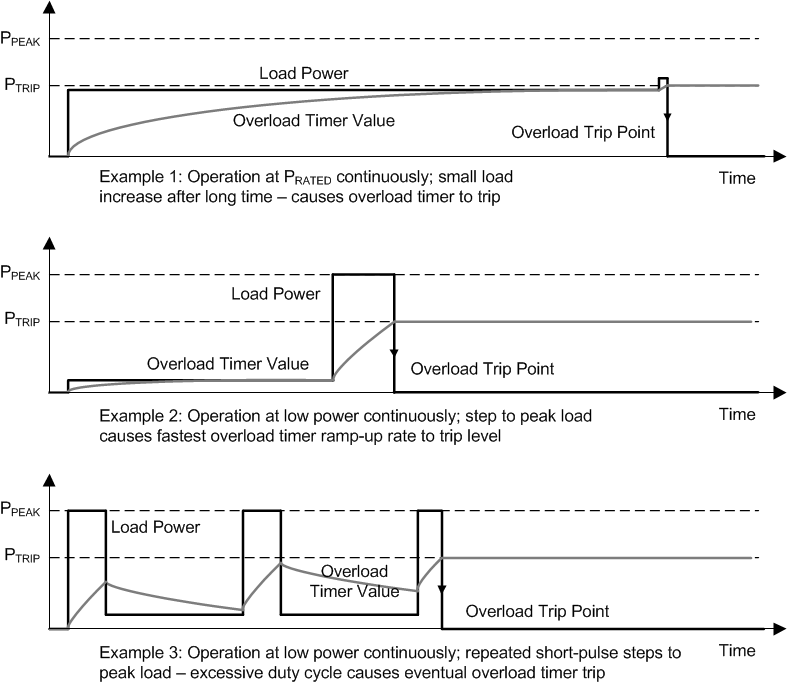 Figure 34. Overload Timer Example Waveforms Under Various Load Scenarios
 Figure 35. Overload Timer Block Diagram
8.3.13 Overload Timer Adjustment (UCC28630 only)
The UCC28630 overload timer trip level and time constant are both selectable from a defined list of combinations. The user can select the overload timer trip level as a percentage of the rated continuous nominal power, PNOM (see Figure 41), and the timer response speed. The available choices are detailed in Table 2.
Table 2. Overload Timer Adjustment
| RPROG PROGRAMMING RESISTOR (kΩ) (E96 series values) |
TIMER CONTINUOUS OPERATION PTRIP/PNOM (%) | TIME CONSTANT AT 200% of PNOM OR IN CC MODE (ms) |
|---|---|---|
| Open, or > 47 | 160 | 1000 |
| 20.0 | 160 | 500 |
| 12.7 | 160 | 150 |
| 9.31 | 135 | 1000 |
| 7.32 | 135 | 500 |
| 6.04 | 135 | 150 |
| 5.11 | 110 | 1000 |
| 4.42 | 110 | 500 |
| 3.92 | 110 | 150 |
The desired pull-down resistance on the DRV pin sets the required overload parameters, as shown in Figure 36. The controller measures the resistance value on the DRV pin at start-up using a low-level test voltage (400 mV to ensure it is well below the lowest possible power MOSFET gate threshold voltage) and sensing the current that flows. Thus, based on the resistance RPROG, the required set of timer parameters can be chosen.
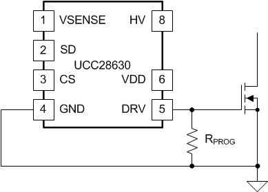 Figure 36. Overload Timer Setting Adjustment
 (with programming pull-down resistor on DRV pin)
To ensure that the sensed current does not sit close to an interval boundary, the resistor values listed in Table 2 (or the closest value possible) should be used. These recommended resistor values position the test current in the center of each interval.
8.3.14 CC-Mode IOUT(lim) Adjustment
For the UCC28631, UCC28632, UCC28633 and UCC28634, the pull-down programming resistor on the DRV pin, as shown in Figure 36, sets the desired CC-Mode limit. The available CC-Mode levels are listed in Table 3, where the CC limit is given as a percentage of the maximum allowed value from Equation 20.
8.3.15 Fault Protections
The controller has several built-in fault protections. Most faults are subject to internal persistence filtering to avoid false-tripping due to noise or spurious glitches from external events. When a fault is detected and persists for the corresponding filter delay time, the device terminates and disables the PWM drive signal. No PWM activity occurs if the fault (pin faults for example) is detected at start-up . Table 4 lists all fault sources, persistence delays and the associated response (latching or auto-restart).
In the case of auto-restart (sometimes called hiccup-mode) faults, the device enters low-power mode for a time period of tRESET(long) (or tRESET(short) in the case of AC line UV fault and X-capacitor discharge), then discharges the VDD pin to the VDD(reset) level, followed by a restart attempt. The device continues in a repeating shutdown-delay-restart loop until the fault is removed. Once the fault clears, the controller restarts automatically, there is no need to remove and re-apply AC input voltage to the system.
Latching faults do not allow any PWM restart attempts until the AC input voltage is removed. In this case the controller enters low-power mode. During low-power mode, the device regulates the VDD pin between two levels VDD(latch_hi) and VDD(latch_lo), as given in Table 7, using the start-up HV current source. This regulation keeps the controller biased to maintain the latched fault condition as long as AC voltage is present at the input. When the device loses AC input voltage during latched-fault mode, the controller resets, and restarts when the AC input is re-applied.
If there is an open-feedback fault due to an open or short on the VSENSE pin or associated external resistor divider on the aux winding, the output voltage is protected against an over-voltage condition. If the open-feedback fault occurs before power-up, the fault will be detected by VSENSE pin- fault protection (see next section 9.3.16), and the controller will not generate any PWM drive signal. This prevents any possible output OV due to this open-feedback fault condition. If the open-feedback occurs after power-up, when the power stage is already operating, the open-feedback condition can cause Vout to increase. In this case, the VDD level will also increase in proportion to Vout (they will track based on the Flyback transformer turns ratio). When the VDD rail reaches the VDD(ovp) protection threshold, the PWM will be disabled, and the controller will go to fault mode, as described above. The VDD(ovp) protection is used as an indirect back-up OV protection mechanism for the main output under running open-feedback fault conditions. The level of output OV depends on the ratio of the normal VDD regulation level to the VDD(ovp) level. Note that UCC28630/1/2/3 use VDD(ovp) trip level of 17.5 V nominal, whereas the UCC28634 uses a lower VDD(ovp) of 14.85 V nominal, to ensure a lower/tighter level of output OV under VSENSE open-feedback conditions. As a result, the user must be careful to choose the number of turns in the transformer aux winding to ensure that the normal VDD regulation is below the VDD(ovp) protection level, to avoid false-triggering of the VDD(ovp) protection.
Table 4. Fault Sources and Associated Responses
| FAULT TYPE | TYPICAL CAUSE | FILTER DELAY TIME | RESPONSE | ||
|---|---|---|---|---|---|
| UCC28630 | UCC28631, UCC28632, UCC28633 | UCC28634 | |||
| VDD OV | Excessive transformer leakage; system board fault | 125 μs (1) | Latching | Auto-restart | Auto-restart |
| VDD UV | Insufficient VDD capacitor; system board fault | 125 μs (1) | Auto-restart | Auto-restart | Auto-restart |
| AC brownout | AC voltage removal or extended dip | 40 ms | Auto-restart | Auto-restart | Auto-restart |
| OverTemp | Internal TJ(max) reached | 125 μs (1) | Latching | Auto-restart | Auto-restart |
| SD pin low | External NTC over-temperature event | 125 μs (1) | Latching | Auto-restart | Auto-restart |
| Overload timer | Excessive load power for too long | Programmable (2) | Auto-restart | N/A | N/A |
| Output OV | System board fault; system output voltage back-driven excessively | 125 μs (1) | Latching | Auto-restart | Auto-restart |
| VSENSE pin | Short or open detected at start-up | No filter (3) | Latching | Latching | Auto-restart |
| DRV pin | Short detected at start-up | No filter (3) | Latching | Latching | Auto-restart |
| CS pin | Short or open detected at start-up | No filter (3) | Latching | Latching | Auto-restart |
| Internal fault | Internal chip diagnostics fault detected | No filter (3) | Latching | Latching | Auto-restart |
8.3.16 Pin-Fault Detection and Protection
The controller includes protection against most practical pin faults. These faults include open pins, pins shorted to adjacent pins, pins shorted to GND and pins shorted to VDD. The device performs pin fault checking at start-up, before the PWM is enabled. Table 5 summarizes the response to pin faults. Most faults cause either a latched shut-down, or failure to start-up. For UCC28634, all pin-faults are non-latching.
A short-circuit from the HV pin (pin 8) to the VDD pin (pin 6) is unlikely to occur, because pin 7 is not included in the package. The HV pin and tracking requires additional PCB spacing in any event to meet creepage requirements. However, if such a fault does occur, the device continues to charge the VDD capacitor through the HV pin external series resistor, and the power supply starts up and appears to operate normally. But because the HV and VDD pins are shorted, the internal HV current source cannot switch-out the external HV resistor, so it always dissipates power. This condition results in a large increase in no-load standby power. A 200-kΩ external HV resistor, dissipates 66 mW at 115 VAC, and 265 mW at 230 VAC. At load levels where the X-capacitor discharge function is operational, the short to VDD appears to be an AC-disconnect event, and causes the device to cycle on and off.
Table 5. Pin Faults and Associated Responses
| PINS | OPEN | ADJACENT SHORT | GND SHORT | VDD SHORT | |
|---|---|---|---|---|---|
| NAME | NO. | ||||
| VSENSE | 1 | Latched fault | Latched fault | Latched fault | No start-up |
| SD | 2 | Normal operation | Latched fault | Latched fault | Latched fault |
| CS | 3 | Latched fault | Latched fault | Latched fault | No start-up |
| GND | 4 | Device fails, power supply damaged | Latched fault | N/A | No start-up |
| DRV | 5 | Hiccup fault | No start-up | Latched fault | No start-up |
| VDD | 6 | No start-up | No start-up | No start-up | N/A |
| no pin | 7 | N/A | N/A | N/A | N/A |
| HV | 8 | No start-up | N/A | No start-up | Fault not detected/Hiccup fault |
8.3.17 Over-Temperature Protection
The controller has built-in thermal protection. If the controller junction enters an over-temperature condition, the controller shuts down. The fault response (latching or auto recovery) depends on the device variant, per Table 4. There is 10°C hysteresis in the over-temperature trip point, the controller only restarts if the junction temperature has dropped by at least 10°C below the trip level.
8.3.18 External Fault Input
An external fault input signal may be applied to the controller SD (shutdown) pin. This signal forces the controller into fault mode. To trigger the fault, the voltage on this pin should be pulled below the fault trip threshold. A typical application is shown in Figure 37, where this pin is used to shut down the controller in the event of an over-temperature event as detected by a NTC (negative temperature coefficient) thermistor. The device pulls up the SD pin internally using a current source. As temperature rises, the external NTC resistance decreases, reducing the voltage on the pin. When the pin voltage drops to the fault trip threshold, the controller enters fault mode. The fault response (latching or recovery) depends on the device variant, per Table 4.
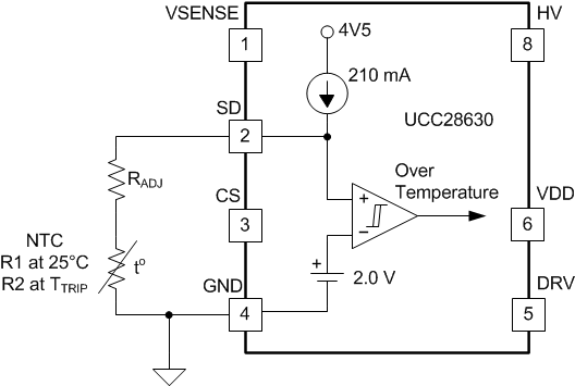 Figure 37. Fault Interface to SD Pin
The required trip resistance can be calculated from the internal trip voltage and pull-up current source. Nominally, this is 9.5 kΩ. Choose the NTC should so that it can achieve this value of resistance at the desired hot-spot trip temperature. If the NTC resistance is too low at the required trip temperature, connect a standard chip resistor in series to bring the total resistance up to 9.5 kΩ.
The device internally filters the SD pin with persistence delay as listed in Table 4. An external filter capacitor is not normally necessary. However, if an application uses an external filter capacitor, the value should be limited to 1 nF maximum. A larger value may impact the useful life of the controller.
8.3.19 External SD Pin Wake Input (except UCC28633)
During low-power modes (when fSW < fSMP(max)), the device disables the internal pull-up on the SD pin. This action allows the pin voltage to fall to GND, and the SD pin then functions as a transient wake-up input. In this case, if the pin rises above the wake threshold while the device is in low-power sleep mode, the device wakes and starts PWM pulses immediately. This feature is useful for applications that require a faster response to load transients from zero or near-zero load, where a wake-up signal can be appropriately coupled to the SD pin from the secondary side.
Figure 38 describes a typical secondary-side wake circuit and coupling of the wake signal to the controller on the primary side. This circuit uses a TL103W component which is an integrated reference plus two op-amps in a convenient SOIC-8 package. Both op-amps are connected to the same internal 2.5-V TL431 type reference, with a 3-resistor divider chain allowing each op-amp to monitor a different level. The upper op-amp output is low as long as the device is regulating the output voltage normally. If a sufficiently large load transient occurs while the primary-side controller is in sleep mode, the output voltage drops below a transient wake level. The upper op-amp output goes high, driving current through the low-cost wake signal opto-coupler. On the primary side, the wake opto-coupler pulls up the SD pin above the wake threshold and forces PWM switching as a reaction to the load transient.
The lower op-amp section monitors the output voltage and its output goes low only when the output voltage is above a minimum enable threshold for the secondary-side wake-up monitor. This action is necessary so that under certain conditions, such as a start-up sequence or short-circuit condition (when the output voltage is already below the transient wake level) that the secondary-side circuit does not continually drive the wake opto-coupler, which could activate an SD pin fault during pin-fault checking at start-up.
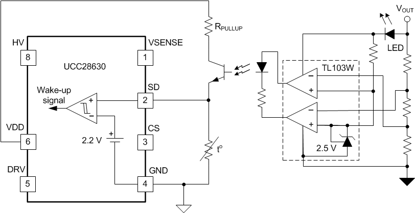 Figure 38. Typical Secondary-Side Voltage Monitor and Wake-Up Circuit for Interfacing to the SD Pin
8.3.20 External Wake Input at VSENSE Pin (UCC28633 Only)
The UCC28633 device variant supports fast PSR transient response via the VSENSE pin. When the loop demand drives the modulator frequency below approximately fSMP(max), the controller enters a low-power sleep mode for a portion of the switching cycle. The sleep interval varies, depending on the switching frequency commanded. The sleep interval is longer for lower switching frequency, and longest at fSW(min). For conventional PSR controllers, if a load transient occurs during this sleep interval, the controller will not react until the next timed wake-up, during which the output voltage can drop significantly, depending on the size of the load step and the amount of output capacitance.
The UCC28633 can respond to fast transient wake signal coupled to the VSENSE pin. If the wake signal exceeds an internal pin threshold VSENSE(wake) while the controller is in sleep mode, the sleep interval is terminated and PWM activity commences within a typical delay time of tWAKE. This dramatically improves the response to heavy load transients from zero load, or very light load. If the switching frequency is above fSMP(max), the controller never enters sleep mode, so wake response on the VSENSE pin never enabled. The commencement of any sleep interval in the controller is delayed until the resonant ringing on the VENSE pin has decreased below the VSENSE(wake) threshold for at least 2 µs. Once the ringing has decreased, the wake response is enabled, and the sleep interval commences.
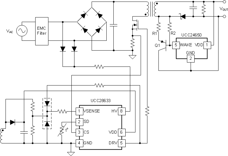
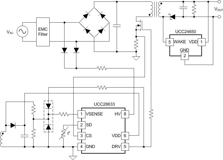 Figure 39. UCC24650 Secondary-Side Voltage Monitor and Wake-Up Circuit
The wake signal at the VSENSE pin can be generated using a secondary side low power voltage monitor such as UCC24650, as shown in Figure 39. Further details can be found in the datasheet for UCC24650. This secondary-side monitor uses the switching activity on the secondary winding to trigger refresh of an internal sample-and-hold circuit to measure and record the system output voltage at the VDD pin. Thereafter, if the actual output voltage, sensed at the VDD pin, drops by ΔWAKE% (see UCC24650 detailed datasheet specifications) of the previously sampled value, the WAKE pin is internally pulled low through a current-limited open-drain switch. As shown in Figure 39, the main output rectifier diode is positioned at the return side of the secondary winding, so that the GND-referenced UCC24650 WAKE function can be deployed. In effect, the WAKE pin shorts out the rectifier diode for a short interval (see UCC24650 detailed datasheet specifications), to draw some current from the output capacitor through the transformer secondary winding. This sets up a low-level pulse of current that then rings resonantly in the power circuit magnetizing inductance and parasitic capacitance. The ringing causes a similar ringing voltage waveform on all transformer windings, including the bias/sense winding, which interfaces to the VSENSE pin. If the initial pulse of current drawn by the secondary WAKE pin is sufficient, then the ringing voltage at the VSENSE pin is large enough to exceed the VSENSE(wake) threshold.
The UCC24650 datasheet Application Information section includes details of how to estimate the amplitude of the wake-pulse ringing at the WAKE pin. In some cases, especially at higher rated output power, the transformer magnetizing inductance is lower, while the total switch node capacitance tends to be higher. This reduces the transformer impedance, and can also result in reduced wake pulse amplitude. In these cases, the UCC24650 WAKE pin output can be augmented with an external PNP circuit Q1, R1 and R2, as shown in Figure 40. In this case, when the WAKE pin pulls low, Q1 turns on, and draws more current through the secondary winding. A current limiting resistor R1 is recommended in series with either collector or emitter. Effectively R1 swamps the UCC24650 internal WAKE pin resistance, RWAKE. A pull-up resistor R2 from base to emitter is also required, to ensure that the WAKE pin is adequately pulled up/down during normal switching activity to properly trigger the internal sample and hold on the VDD pin. The external PNP device Q1 must have at least the same voltage rating as the main rectifier diode.
8.3.21 Mode Control and Switching Frequency Modulation
The flyback controller supports applications that require a wide range of operating power levels. This range can include effectively zero output power in standby conditions, up to a maximum rated continuous power, and then beyond this, to a mode of peak operating power for a limited time. The modulator operates in multiple modes to support these power requirements in an efficient way. In some regions, the modulator operates in AM mode at fixed frequency, where the device adjusts the amplitude of the peak current to regulate the output. In other regions, the modulator operates in FM mode at fixed peak current, where the device adjusts the switching frequency to regulate the output. By adjusting only peak current or frequency, (depending on operating region) the control loop smoothly regulates the power flow of the power stage. The shape of the modulator gain curve helps counteract the increasing power stage gain as load is decreased.
In the high-power region of the modulator, the device adjusts both peak current and frequency together, to allow higher power delivery with a modest increase in peak current. In this high-power region, the power stage typically transitions into continuous-conduction mode (CCM), particularly at low line. The combination of up to 2× frequency increase and 1.25× peak current increase in CCM allows up to 2× peak power delivery capability for a given transformer size. Figure 41 provides details regarding the modulator peak current (in mV at the CS pin) and switching frequency variation vs power demand level. The frequency adjusts from a minimum of 200 Hz up to a maximum of 120 kHz. The peak-current sense voltage at the CS pin varies from 172 mV to 800 mV. Table 6 summarizes the modulator breakpoints and corresponding percentage power levels.
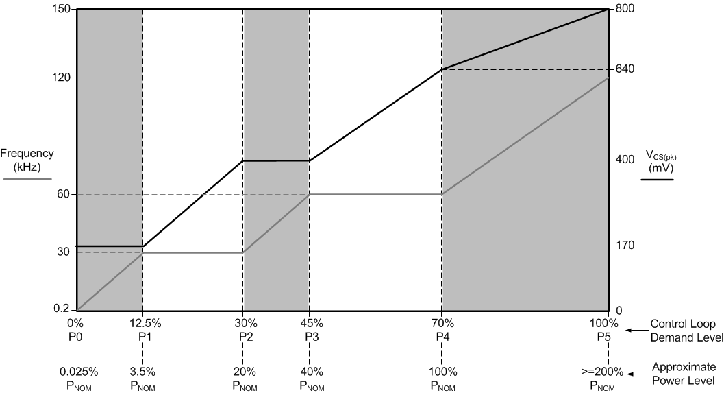 Figure 41. Modulator Modes and Frequency Variations with Power Level
For no load and very light loads (P0 to P1 region) the modulator operates in a pulse frequency modulation (PFM) mode. In PFM mode, the device maintains a constant peak current in the transformer magnetizing inductance, so that the energy transferred in each switching cycle is fixed. The magnetic sensing, fixed-point sampling scheme requires that the device always imposes a minimum peak current. This minimum peak-current demand naturally results in a minimum transformer magnetizing volt-second product that the device maintains across the input line voltage range. Ensuring a minimum on-time magnetizing volt-seconds also ensures a balancing volt-second flyback interval, during which the device guarantees the availability of the output voltage sample. Magnetic Sensing: Power Stage Design Constraints outlines the transformer design constraints necessary to comply with the minimum on-time and minimum required volt-seconds.
In the P0 to P1 region, the energy transfer per switching cycle is maximized, which in turn minimizes the switching frequency and associated switching and drive losses, to improve efficiency. However, due to concerns about audible noise in this region, the peak current VCS(min) in this region is limited to 22% of the peak VCS(max) at the maximum demand level. This peak-current derating maintains the transformer peak flux density to 22% of the peak, to minimize transformer-induced audible noise. Assuming a maximum peak flux density of typically 300 mT at highest peak current, this derating sets the peak flux level at approximately 65 mT in the light-load region. Empirically, this flux level greatly reduces magnetic audible noise for a variety of power levels and transformer designs. In this region, the use of sleep modes (where most of the device internal blocks are powered down in between switching cycles) minimizes the controller power consumption. Minimizing controller power consumption helps reduce total standby power consumption, and also greatly eases the bias design constraints.
For higher loads above P1 (P1 to P2 region), the device fixes the modulator frequency at a low value above the audible range, while the peak switch current ramps up from the minimum level, to deliver the increased output power. Maintaining a fixed low-switching frequency while ramping peak current, minimizes switching losses to provide good light-load efficiency.
For higher loads above P2 (P2 to P3 region), the device maintains a constant peak-switch current, while the modulator frequency ramps to its nominal operating value. The normal heavy load (between 40% and 100% of rated) operating power range lies between P3 and P4. In this region the device maintains a constant switching frequency at the nominal value fSW(nom), and the peak switch current ramps to achieve increased output power. Fixed-frequency operation at nominal operating power results in consistent EMI and transient load step performance.
Table 6. Frequency and Peak-Current Modulator Operating Ranges and Breakpoints
| MODULATOR BREAKPOINT | DEMAND LEVEL (%) | APPROXIMATE POWER LEVEL % of PNOM | VCS PEAK | FREQUENCY fSW | ||
|---|---|---|---|---|---|---|
| (mV) | (kHz) | |||||
| PO0 | 0 | 0.025 | 172 | VCS(min) | 0.200 | fSW(min) |
| PO1 | 12.5 | 3.5 | 172 | VCS(min) | 30 | fSW(LL) |
| PO2 | 30 | 20 | 400 | VCS(nom) | 30 | fSW(LL) |
| PO3 | 45 | 40 | 400 | VCS(nom) | 60 | fSW(nom) |
| PO4 | 70 | 100 | 640 | VCS(bcm) | 60 | fSW(nom) |
| PO5 | 100 | > 200 | 800 | VCS(max) | 120 | fSW(max) |
The peak-power range lies between P4 and P5. In this region the transformer can operate in CCM depending on loading and line voltage. By increasing the frequency appropriately, higher average input current can be processed for the same peak current, so the transformer size does not need to increase substantially for a high-rated transient peak power. The modulator does, however, also increase the peak current in this region of operation, requiring a modest increase in transformer size, but this allows a larger transient peak power to be delivered. The modulator control loop adjusts both the frequency and peak current according to the power demand so that the increased frequency and peak current meets the load demand.
Figure 42 shows the modulator gain curve, specifically the non-linear modulator gain vs load. At very light loads, the modulator gain remains low, to help counteract the effect of the higher power stage gain as the load resistance increases. This low gain helps stabilize the magnetic regulation loop in the light load territory, where the output voltage sample rate drops with decreasing switching frequency. At heavier loads, the modulator gain progressively and smoothly increases to help improve transient response. When the switching frequency increases above the maximum magnetic sense sample rate (fSMP(max)), the magnetic sense voltage control sample rate is clamped.
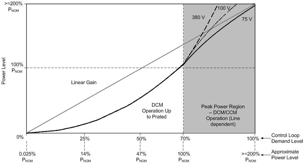 Figure 42. Modulator Gain Curves vs Bulk Capacitor Voltage
8.3.22 Frequency Dither For EMI (except UCC28632)
To help ease EMI compliance of the system, the device dithers the switching frequency over time. This dithering of frequency is active only above the light-load region threshold (PLL(%)) point on the modulator curve. In the light load regions, frequency dither is disabled. The frequency dither follows a repeating pattern, in the sequence:
{(fNOM), (fNOM + 6.7%), (fNOM + 6.7%), fNOM), (fNOM – 6.7%), (fNOM – 6.7%), (fNOM), . . . .}
The controller dwells at each frequency for 1 ms. The pattern repeats every 6 ms, as shown graphically in Figure 43.
NOTE
The device always dithers frequency between 6.7% and –6.7% at every operating point in the modulator. The dither frequency delta is not an absolute delta, it scales with actual operating frequency, depending on the exact operating point value.
 Figure 43. Frequency Dither Pattern Details
In order to balance the power flow and reduce and output ripple as a consequence of frequency dithering, the device automatically adjusts peak-current demand in inverse-proportion to the square-root of the frequency dither deviation. Thus, since the power flow (in DCM) is given by (½ × L × I2 × fSW), this balances the power flow, and cancels the output ripple as a consequence of frequency dithering.
8.4 Device Functional Modes
8.4.1 Device Internal Key Parameters
The application designer requires some key device internal parameters in order to calculate the required power stage components and values for a given design specification . Table 7 summarizes the key parameters.

 for AC connection and VIN(avg) = VRMS x √2 for DC connection
