SLLA631A December 2023 – January 2024 UCC21220 , UCC21222-Q1 , UCC21520 , UCC21520-Q1 , UCC21530 , UCC21530-Q1 , UCC21540 , UCC21540-Q1
- 1
- Abstract
- Trademarks
- 1Introduction
- 2When Can Extreme Narrow Input Pulses Happen in a Power Stage?
- 3How Narrow Input Pulse Widths Threaten the Gate Driver
- 4Which System Factors Can Influence the Result
- 5How do you Know Whether Your System Should Limit Narrow Pulses?
- 6Summary
- 7References
- 8Revision History
1 Introduction
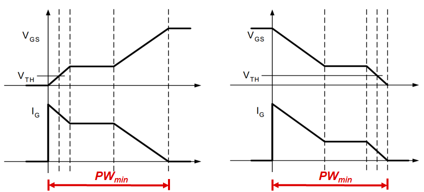
A typical MOSFET turn-on and turn-off periods are shown in Figure 1-1. The goal for the gate driver is to reach a given MOSFET’s target gate-to-source voltage (VGS) by charging up the gate of the MOSFET, through a minimum gate threshold voltage (VTH) and apply the maximum drive strength during the miller plateau region to charge the gate to the maximum drive voltage. A complete transition is achieved when the target VGS is met and no gate current (IG) flows to charge the external load. This defines the minimum pulse width, PWmin, for an ON-transition. For an OFF-transition, the procedure goes in reverse but the defined minimum pulse width is when VGS = 0V and IG = 0A. Zero Current Switching (ZCS) is achieved when IG = 0A and is the good target when transitioning between ON/OFF or OFF/ON transitions for the gate driver.
 Figure 1-1 MOSFET Gate Turn ON and OFF Period
| Parameter | Test Condition | MIN | TYP | MAX | UNIT | |
|---|---|---|---|---|---|---|
| tRISE | Output rise , 20% 80% measured points | Cout= 1.8nF | 6 | 16 | ns | |
| tFALL | Output fall time, 90% to 10% measured points | Cout= 1.8nF | 7 | 12 | ns | |
| tPWmin | Minimum pulse width | Output off for less than minimum Cout= 0pF | 20 | ns | ||
It is important to note that the minimum pulse width specification in a data sheet only describes the ability of an UNLOADED driver (COUT=0pF) to produce an output pulse from an input of at least the specified width and is not an indication of the pulse minimum width for robust, reliable operation for the gate driver.
A typical application can have a load on the gate driver and often operates at the recommended maximum VDD voltage. Under these conditions, the minimum pulse required by the driver IC can be 4 to 5 times larger than this specification defined at no load.
Each application can have a different minimum pulse width that can be reliably applied to the gate driver. There are a few variables that can impact the minimum pulse that can be applied. These factors include: the gate capacitance, VDD supply voltage, series resistance ( RG), peak current (Ipk), and PCB layout parasitic.