SPRACP4A December 2019 – June 2024 AM67 , AM67A , AM68 , AM68A , AM69 , AM69A , DRA821U , DRA821U-Q1 , DRA829J , DRA829J-Q1 , DRA829V , DRA829V-Q1 , TDA4AEN-Q1 , TDA4AH-Q1 , TDA4AL-Q1 , TDA4AP-Q1 , TDA4APE-Q1 , TDA4VE-Q1 , TDA4VEN-Q1 , TDA4VH-Q1 , TDA4VL-Q1 , TDA4VM , TDA4VM-Q1 , TDA4VP-Q1 , TDA4VPE-Q1
- 1
- Abstract
- Trademarks
- 1Introduction
-
2High-Speed Interface Design Guidance
- 2.1 Trace Impedance
- 2.2 Trace Lengths
- 2.3 Differential Signal Length Matching
- 2.4 Signal Reference Planes
- 2.5 Differential Signal Spacing
- 2.6 Additional Differential Signal Rules
- 2.7 Symmetry in the Differential Pairs
- 2.8 Connectors and Receptacles
- 2.9 Via Discontinuity Mitigation
- 2.10 Back-Drill Via Stubs
- 2.11 Via Anti-Pad Diameter
- 2.12 Equalize Via Count
- 2.13 Surface-Mount Device Pad Discontinuity Mitigation
- 2.14 Signal Bending
- 2.15 ESD and EMI Considerations
- 2.16 ESD and EMI Layout Rules
- 3Interface-Specific Design Guidance
- 4Board Design Simulations
- 5References
- 6Revision History
2.3 Differential Signal Length Matching
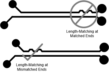
Match the etch lengths of the relevant differential pair traces. Intra-pair skew is the term used to define the difference between the etch length of the + and – lane of a differential pair. Inter-pair skew is used to describe the difference between the etch lengths of a differential pair from another differential pair of the same group. The etch length of the differential pair groups do not need to match. For example the etch lengths of USB 3.0 TX and RX do not need to match. There are also standards that do not have a Interpair skew requirement because the different lanes do not have to be the same length. When matching the intra-pair skew of the high-speed signals, add serpentine routing to match the lengths as close to the mismatched ends as possible, see Figure 2-1.
 Figure 2-1 Differential Pair Length Matching