SPRACP4A December 2019 – June 2024 AM67 , AM67A , AM68 , AM68A , AM69 , AM69A , DRA821U , DRA821U-Q1 , DRA829J , DRA829J-Q1 , DRA829V , DRA829V-Q1 , TDA4AEN-Q1 , TDA4AH-Q1 , TDA4AL-Q1 , TDA4AP-Q1 , TDA4VE-Q1 , TDA4VEN-Q1 , TDA4VH-Q1 , TDA4VL-Q1 , TDA4VM , TDA4VM-Q1 , TDA4VP-Q1
- 1
- Abstract
- Trademarks
- 1Introduction
-
2High-Speed Interface Design Guidance
- 2.1 Trace Impedance
- 2.2 Trace Lengths
- 2.3 Differential Signal Length Matching
- 2.4 Signal Reference Planes
- 2.5 Differential Signal Spacing
- 2.6 Additional Differential Signal Rules
- 2.7 Symmetry in the Differential Pairs
- 2.8 Connectors and Receptacles
- 2.9 Via Discontinuity Mitigation
- 2.10 Back-Drill Via Stubs
- 2.11 Via Anti-Pad Diameter
- 2.12 Equalize Via Count
- 2.13 Surface-Mount Device Pad Discontinuity Mitigation
- 2.14 Signal Bending
- 2.15 ESD and EMI Considerations
- 2.16 ESD and EMI Layout Rules
- 3Interface-Specific Design Guidance
- 4Board Design Simulations
- 5References
- 6Revision History
3.4.1 CSI-2®, DSI® Interface Schematic
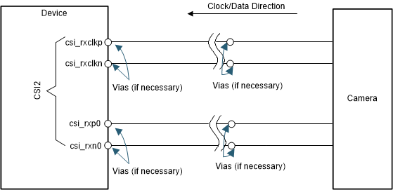
The CSI-2 schematics vary, depending on the number of lanes implemented. Depending upon device, each CSI-2 can include up to four data lanes. General connectivity is straightforward and consistent between implementations. Figure 3-8 illustrates a CSI-2 system using a single lane.
 Figure 3-8 CSI-2® High-Level
Schematic
Figure 3-8 CSI-2® High-Level
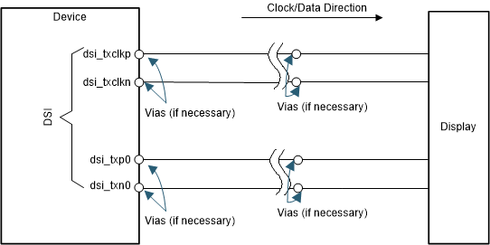
SchematicThe DSI schematics vary, depending on the number of lanes implemented. Depending upon device, each DSI can include up to four data lanes. General connectivity is straightforward and consistent between implementations. Figure 3-9 illustrates a DSI system using a single lane.
 Figure 3-9 DSI High-Level
Schematic