SPRACP4A December 2019 – June 2024 AM67 , AM67A , AM68 , AM68A , AM69 , AM69A , DRA821U , DRA821U-Q1 , DRA829J , DRA829J-Q1 , DRA829V , DRA829V-Q1 , TDA4AEN-Q1 , TDA4AH-Q1 , TDA4AL-Q1 , TDA4AP-Q1 , TDA4APE-Q1 , TDA4VE-Q1 , TDA4VEN-Q1 , TDA4VH-Q1 , TDA4VL-Q1 , TDA4VM , TDA4VM-Q1 , TDA4VP-Q1 , TDA4VPE-Q1
- 1
- Abstract
- Trademarks
- 1Introduction
-
2High-Speed Interface Design Guidance
- 2.1 Trace Impedance
- 2.2 Trace Lengths
- 2.3 Differential Signal Length Matching
- 2.4 Signal Reference Planes
- 2.5 Differential Signal Spacing
- 2.6 Additional Differential Signal Rules
- 2.7 Symmetry in the Differential Pairs
- 2.8 Connectors and Receptacles
- 2.9 Via Discontinuity Mitigation
- 2.10 Back-Drill Via Stubs
- 2.11 Via Anti-Pad Diameter
- 2.12 Equalize Via Count
- 2.13 Surface-Mount Device Pad Discontinuity Mitigation
- 2.14 Signal Bending
- 2.15 ESD and EMI Considerations
- 2.16 ESD and EMI Layout Rules
- 3Interface-Specific Design Guidance
- 4Board Design Simulations
- 5References
- 6Revision History
3.1.2 Routing Specifications
These parameters are recommendations only, intended to get the design close to success prior to simulation. To make sure the PCB design meets all requirements, it is required that the design be simulated and those results compared with the simulation results defined in Section 4.
| Parameter | MIN | TYP | MAX | Unit |
|---|---|---|---|---|
| USB3.1 Gen1 Operating Speed (Super Speed signals) | 2.5 (1) | GHz | ||
| USB3.1 Signal Trace Length | 5000 (2) | Mils | ||
| USB3.1 Differential Pair Skew | 1 | ps | ||
| USB3.1 Differential Impedance | 85.5 | 90 | 94.5 | Ω |
| Number of stubs allowed on USB3.1 traces | 0 | stubs | ||
| Number of vias on each USB3.1 trace | 2 | Vias | ||
| Via Stub Length (3) | 20 | Mils | ||
| USB3.1 Differential Pair to any other Trace Spacing (4) | 2×DS | 3×DS |
| Parameter | MIN | TYP | MAX | Unit |
|---|---|---|---|---|
| USB2.0 Operating Speed | 240 | MHz | ||
| USB2.0 Signal Trace Length | 7000 (1) | Mils | ||
| USB2.0 Differential Pair Skew | 5 | ps | ||
| USB2.0 Differential Impedance | 81 | 90 | 99 | Ω |
| Number of stubs allowed on USB2.0 traces | 0 | stubs | ||
| Number of vias on each USB2.0 trace | 4 | Vias | ||
| USB2.0 Differential Pair to any other Trace Spacing (2) | 2×DS | 3×DS |
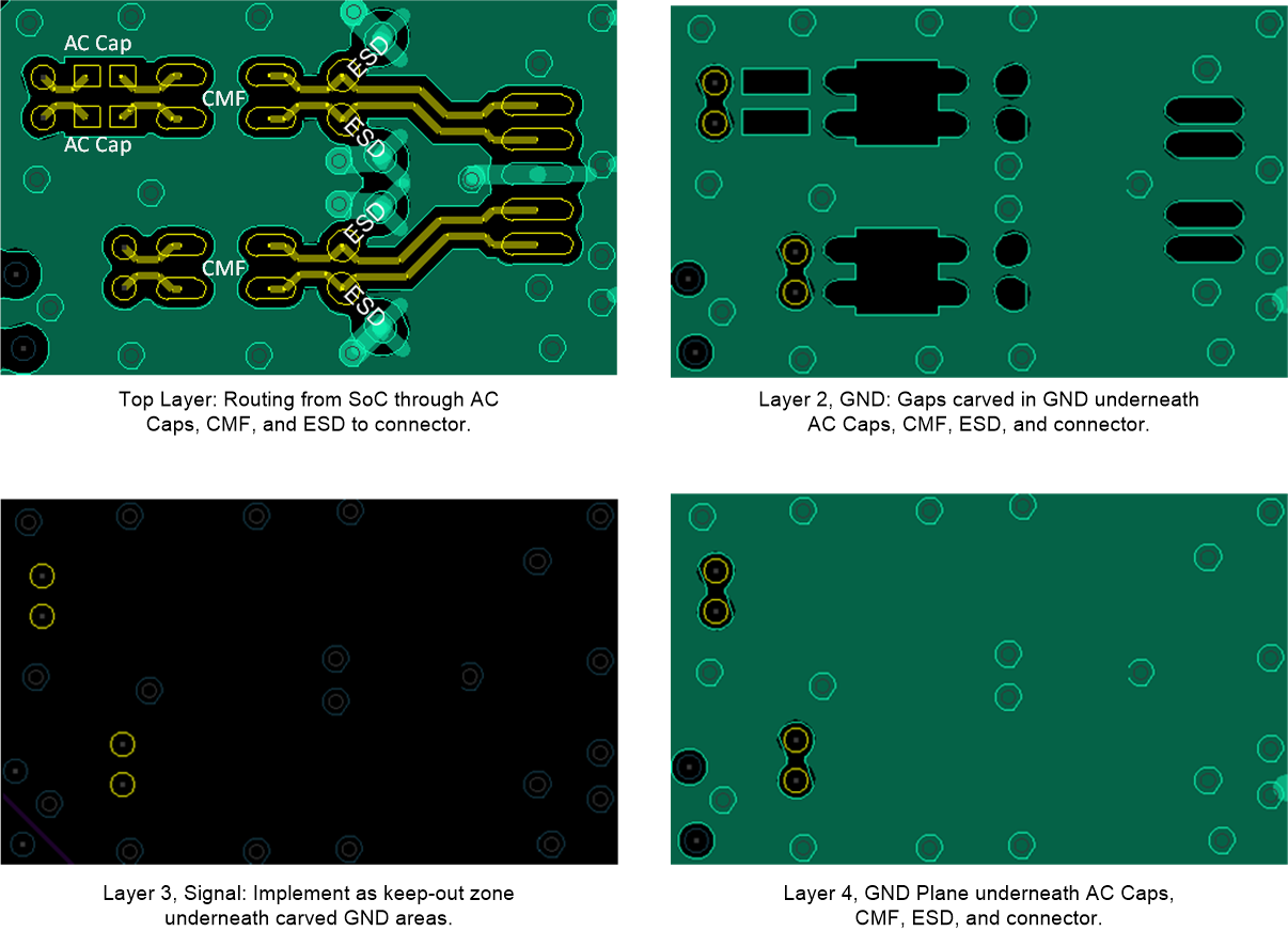
Component pads create impedance discontinuities due to the increased widths of the pads. In an effort to minimize impedance discontinuities, voids are created in the reference plane beneath the component pads. Figure 3-3 presents an example layout, demonstrating the “carve GND” concept. Before and after effects of the reference plane voids can be seen in TDR plots and simulation results.
 Figure 3-3 USB 3.1 Example “carve GND” Layout