SPRACP4A December 2019 – June 2024 AM67 , AM67A , AM68 , AM68A , AM69 , AM69A , DRA821U , DRA821U-Q1 , DRA829J , DRA829J-Q1 , DRA829V , DRA829V-Q1 , TDA4AEN-Q1 , TDA4AH-Q1 , TDA4AL-Q1 , TDA4AP-Q1 , TDA4APE-Q1 , TDA4VE-Q1 , TDA4VEN-Q1 , TDA4VH-Q1 , TDA4VL-Q1 , TDA4VM , TDA4VM-Q1 , TDA4VP-Q1 , TDA4VPE-Q1
- 1
- Abstract
- Trademarks
- 1Introduction
-
2High-Speed Interface Design Guidance
- 2.1 Trace Impedance
- 2.2 Trace Lengths
- 2.3 Differential Signal Length Matching
- 2.4 Signal Reference Planes
- 2.5 Differential Signal Spacing
- 2.6 Additional Differential Signal Rules
- 2.7 Symmetry in the Differential Pairs
- 2.8 Connectors and Receptacles
- 2.9 Via Discontinuity Mitigation
- 2.10 Back-Drill Via Stubs
- 2.11 Via Anti-Pad Diameter
- 2.12 Equalize Via Count
- 2.13 Surface-Mount Device Pad Discontinuity Mitigation
- 2.14 Signal Bending
- 2.15 ESD and EMI Considerations
- 2.16 ESD and EMI Layout Rules
- 3Interface-Specific Design Guidance
- 4Board Design Simulations
- 5References
- 6Revision History
3.5.1 UFS Interface Schematic
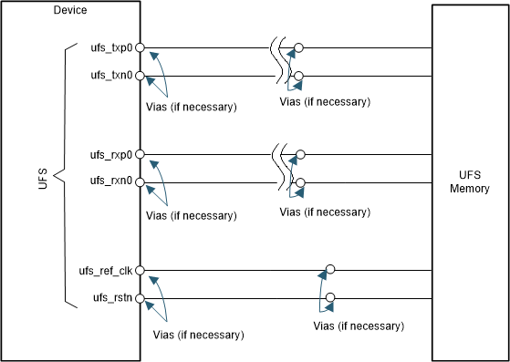
The UFS interface schematics vary, depending on the number of lanes implemented, as depending if the memory is embedded or removable. Depending upon the device, each UFS interface can include up to two data lanes (each direction). General connectivity is straightforward and consistent between implementations. Figure 3-10 illustrates a UFS system using a single lane. The TX and RX signals are implemented as differential pairs. The REF_CLK and RSTN signals are single-ended signals. These single ended are slow speed interfaces, and nothing special is required for PCB layout of these signals.
 Figure 3-10 UFS Interface High Level
Schematic