SPRACP4A December 2019 – June 2024 AM67 , AM67A , AM68 , AM68A , AM69 , AM69A , DRA821U , DRA821U-Q1 , DRA829J , DRA829J-Q1 , DRA829V , DRA829V-Q1 , TDA4AEN-Q1 , TDA4AH-Q1 , TDA4AL-Q1 , TDA4AP-Q1 , TDA4VE-Q1 , TDA4VEN-Q1 , TDA4VH-Q1 , TDA4VL-Q1 , TDA4VM , TDA4VM-Q1 , TDA4VP-Q1
- 1
- Abstract
- Trademarks
- 1Introduction
-
2High-Speed Interface Design Guidance
- 2.1 Trace Impedance
- 2.2 Trace Lengths
- 2.3 Differential Signal Length Matching
- 2.4 Signal Reference Planes
- 2.5 Differential Signal Spacing
- 2.6 Additional Differential Signal Rules
- 2.7 Symmetry in the Differential Pairs
- 2.8 Connectors and Receptacles
- 2.9 Via Discontinuity Mitigation
- 2.10 Back-Drill Via Stubs
- 2.11 Via Anti-Pad Diameter
- 2.12 Equalize Via Count
- 2.13 Surface-Mount Device Pad Discontinuity Mitigation
- 2.14 Signal Bending
- 2.15 ESD and EMI Considerations
- 2.16 ESD and EMI Layout Rules
- 3Interface-Specific Design Guidance
- 4Board Design Simulations
- 5References
- 6Revision History
3.1.1.1 Support Components
AC coupling capacitors are required on the transmit Super Speed data pairs. Table 3-1 shows the requirements for these capacitors.
| Parameter | MIN | TYP | MAX | Unit |
|---|---|---|---|---|
| PCIe AC coupling capacitor value | 175 | 220 | 265 | nF |
| PCIe AC coupling capacitor package size | 0402 | 0603 | EIA (1),(2) |
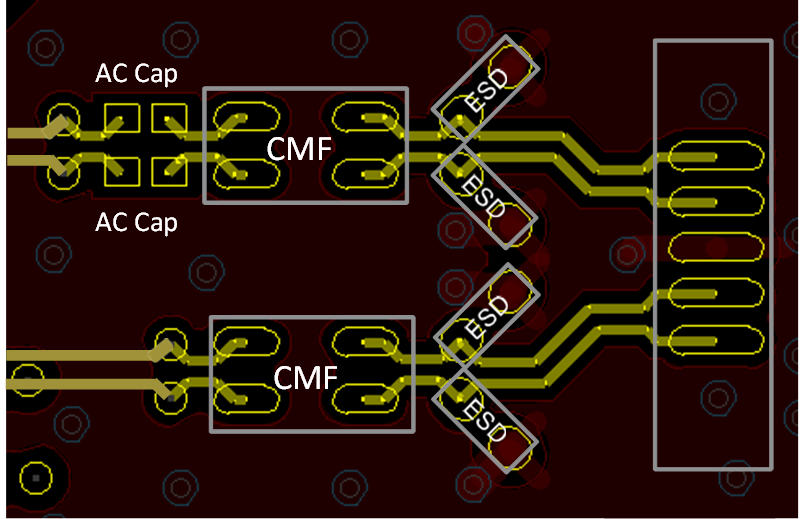
A typical USB interface may also common mode chokes for suppression of high-frequency noise. Because USB can interface to off-board peripherals, ESD protection is also included in the example.
| Device | Supplier | Part Number | Comment |
|---|---|---|---|
| ESD | TI | TDP1E05U06 | Minimize Capacitance |
| CMF | Murata | DLW21SZ900HQ2 | Support Target Data Rates |
Figure 3-2 shows the placement diagram for USB 3.1 Super Speed signals.
 Figure 3-2 USB 3.1
Super Speed Placement Diagram