SPRACP4A December 2019 – June 2024 AM67 , AM67A , AM68 , AM68A , AM69 , AM69A , DRA821U , DRA821U-Q1 , DRA829J , DRA829J-Q1 , DRA829V , DRA829V-Q1 , TDA4AEN-Q1 , TDA4AH-Q1 , TDA4AL-Q1 , TDA4AP-Q1 , TDA4VE-Q1 , TDA4VEN-Q1 , TDA4VH-Q1 , TDA4VL-Q1 , TDA4VM , TDA4VM-Q1 , TDA4VP-Q1
- 1
- Abstract
- Trademarks
- 1Introduction
-
2High-Speed Interface Design Guidance
- 2.1 Trace Impedance
- 2.2 Trace Lengths
- 2.3 Differential Signal Length Matching
- 2.4 Signal Reference Planes
- 2.5 Differential Signal Spacing
- 2.6 Additional Differential Signal Rules
- 2.7 Symmetry in the Differential Pairs
- 2.8 Connectors and Receptacles
- 2.9 Via Discontinuity Mitigation
- 2.10 Back-Drill Via Stubs
- 2.11 Via Anti-Pad Diameter
- 2.12 Equalize Via Count
- 2.13 Surface-Mount Device Pad Discontinuity Mitigation
- 2.14 Signal Bending
- 2.15 ESD and EMI Considerations
- 2.16 ESD and EMI Layout Rules
- 3Interface-Specific Design Guidance
- 4Board Design Simulations
- 5References
- 6Revision History
2.11 Via Anti-Pad Diameter
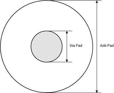
Via transitions can be significant sources of impedance variation along the trace. The anti-pad size of the via across different layers also needs to be adjusted to make sure that the impedance is maintained at a uniform value. Too large an anti-pad leads to an inductive effect and a corresponding increase in the trace impedance, while too small an anti-pad similarly results in a capacitive effect and a dip in the overall trace impedance. The copper clearance, indicated by this anti-pad, must be met on all layers where the via exists, including both routing layer and plane layers. The traces connecting to the via barrel contain the only copper allowed in this area; non-functional or unconnected via pads are not permitted. For an example of a via anti-pad diameter, see Figure 2-13.
 Figure 2-13 Example of Via Anti-Pad