SPRACP4A December 2019 – June 2024 AM67 , AM67A , AM68 , AM68A , AM69 , AM69A , DRA821U , DRA821U-Q1 , DRA829J , DRA829J-Q1 , DRA829V , DRA829V-Q1 , TDA4AEN-Q1 , TDA4AH-Q1 , TDA4AL-Q1 , TDA4AP-Q1 , TDA4APE-Q1 , TDA4VE-Q1 , TDA4VEN-Q1 , TDA4VH-Q1 , TDA4VL-Q1 , TDA4VM , TDA4VM-Q1 , TDA4VP-Q1 , TDA4VPE-Q1
- 1
- Abstract
- Trademarks
- 1Introduction
-
2High-Speed Interface Design Guidance
- 2.1 Trace Impedance
- 2.2 Trace Lengths
- 2.3 Differential Signal Length Matching
- 2.4 Signal Reference Planes
- 2.5 Differential Signal Spacing
- 2.6 Additional Differential Signal Rules
- 2.7 Symmetry in the Differential Pairs
- 2.8 Connectors and Receptacles
- 2.9 Via Discontinuity Mitigation
- 2.10 Back-Drill Via Stubs
- 2.11 Via Anti-Pad Diameter
- 2.12 Equalize Via Count
- 2.13 Surface-Mount Device Pad Discontinuity Mitigation
- 2.14 Signal Bending
- 2.15 ESD and EMI Considerations
- 2.16 ESD and EMI Layout Rules
- 3Interface-Specific Design Guidance
- 4Board Design Simulations
- 5References
- 6Revision History
2.9 Via Discontinuity Mitigation
A via presents a short section of change in geometry to a trace and can appear as a capacitive discontinuity, an inductive discontinuity, or both. These discontinuities result in reflections and some degradation of a signal as the signal travels through the via. Reduce the overall via stub length to minimize the negative impacts of vias (and associated via stubs).
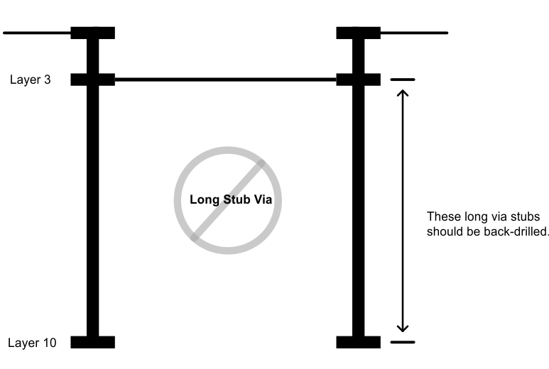
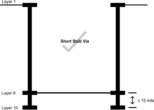
Because longer via stubs resonate at lower frequencies and increase insertion loss, keep these stubs as short as possible. In most cases, the stub portion of the via present significantly more signal degradation than the signal portion of the via. TI recommends keeping via stubs to less than 15mils. Longer stubs must be back-drilled.
For examples of short and long via lengths, see Figure 2-11 and Figure 2-12.
 Figure 2-11 Via
Length (Long Stub)
 Figure 2-12 Via
Length (Short Stub)