SPRACP4A December 2019 – June 2024 AM67 , AM67A , AM68 , AM68A , AM69 , AM69A , DRA821U , DRA821U-Q1 , DRA829J , DRA829J-Q1 , DRA829V , DRA829V-Q1 , TDA4AEN-Q1 , TDA4AH-Q1 , TDA4AL-Q1 , TDA4AP-Q1 , TDA4APE-Q1 , TDA4VE-Q1 , TDA4VEN-Q1 , TDA4VH-Q1 , TDA4VL-Q1 , TDA4VM , TDA4VM-Q1 , TDA4VP-Q1 , TDA4VPE-Q1
- 1
- Abstract
- Trademarks
- 1Introduction
-
2High-Speed Interface Design Guidance
- 2.1 Trace Impedance
- 2.2 Trace Lengths
- 2.3 Differential Signal Length Matching
- 2.4 Signal Reference Planes
- 2.5 Differential Signal Spacing
- 2.6 Additional Differential Signal Rules
- 2.7 Symmetry in the Differential Pairs
- 2.8 Connectors and Receptacles
- 2.9 Via Discontinuity Mitigation
- 2.10 Back-Drill Via Stubs
- 2.11 Via Anti-Pad Diameter
- 2.12 Equalize Via Count
- 2.13 Surface-Mount Device Pad Discontinuity Mitigation
- 2.14 Signal Bending
- 2.15 ESD and EMI Considerations
- 2.16 ESD and EMI Layout Rules
- 3Interface-Specific Design Guidance
- 4Board Design Simulations
- 5References
- 6Revision History
4.5.3 Simulation Methodology
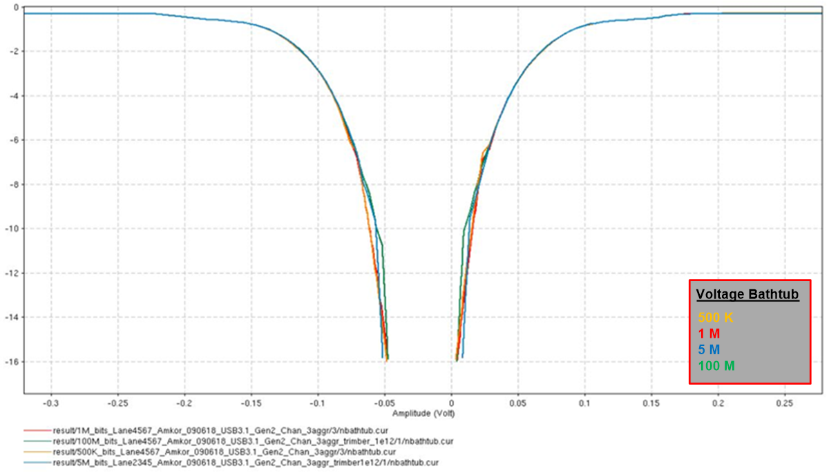
For interfaces where the eye mask is specified in terms of a BER target it is recommended to run the initial channel simulations for around 100K bits and observe the extrapolated bathtub curves for the corresponding target BER, as reported by the simulator. Another simulation for around 500K and 1M bits can be rerun and the bathtub curves can be overlaid to observe the impact of running for larger bit sequences. An example of voltage bathtub curves overlaid is shown in Figure 4-3. Similar overlay can be made for the jitter bathtub curves.
 Figure 4-3 Bathtub Curve Overlay
Typically, all the ISI should be accounted for within the first 100K bits of the simulation and beyond this point, all bathtub curves should converge if the Random Jitter (Rj) in the models is sufficiently small. It is recommended to confirm this convergence up front by running at least one set of system-level channel simulations each for 100K, 500K and 1M bit sequences. If the voltage and jitter bathtub curves from each of these simulations are almost identical, the remainder of the simulations can be run at 100K bits to optimize run times.
For interfaces where the eye mask is not specified for any particular BER target, a 100K bit simulation should suffice.