SPRACP4A December 2019 – June 2024 AM67 , AM67A , AM68 , AM68A , AM69 , AM69A , DRA821U , DRA821U-Q1 , DRA829J , DRA829J-Q1 , DRA829V , DRA829V-Q1 , TDA4AEN-Q1 , TDA4AH-Q1 , TDA4AL-Q1 , TDA4AP-Q1 , TDA4VE-Q1 , TDA4VEN-Q1 , TDA4VH-Q1 , TDA4VL-Q1 , TDA4VM , TDA4VM-Q1 , TDA4VP-Q1
- 1
- Abstract
- Trademarks
- 1Introduction
-
2High-Speed Interface Design Guidance
- 2.1 Trace Impedance
- 2.2 Trace Lengths
- 2.3 Differential Signal Length Matching
- 2.4 Signal Reference Planes
- 2.5 Differential Signal Spacing
- 2.6 Additional Differential Signal Rules
- 2.7 Symmetry in the Differential Pairs
- 2.8 Connectors and Receptacles
- 2.9 Via Discontinuity Mitigation
- 2.10 Back-Drill Via Stubs
- 2.11 Via Anti-Pad Diameter
- 2.12 Equalize Via Count
- 2.13 Surface-Mount Device Pad Discontinuity Mitigation
- 2.14 Signal Bending
- 2.15 ESD and EMI Considerations
- 2.16 ESD and EMI Layout Rules
- 3Interface-Specific Design Guidance
- 4Board Design Simulations
- 5References
- 6Revision History
4.4 Time Domain Reflectometry (TDR) Analysis
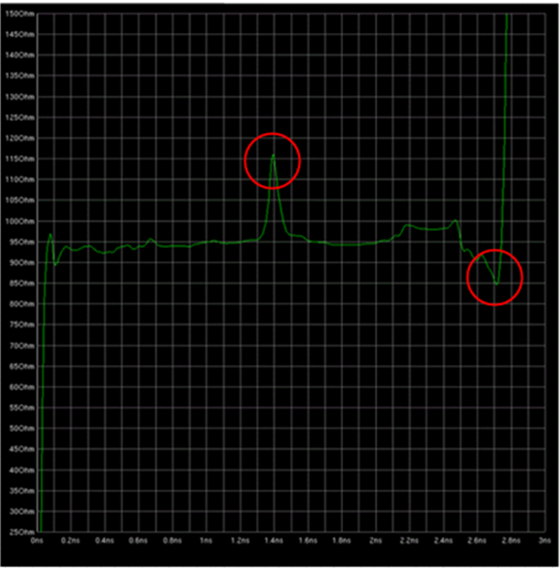
As a lot of the design fixes are targeted towards maintaining uniform trace impedance, an important analysis method used in assessing the quality of the design is the Time Domain Reflectometry (TDR) Analysis. This plots the impedance of a trace as a function of its length. An example of this is shown in Figure 4-1.
 Figure 4-1 TDR Plot Example With Impedance Mismatch
As shown in Figure 4-1 (TDR plot example), the TDR plot highlights impedance discontinuities in the trace from one end to the other. This method depends on a reflected waveform from the far-end of the trace. The delay in the plot corresponding to a particular point in the trace actually corresponds to 2 times the distance of that point from the source, owing to the round trip time. This needs to be factored in for assessing the source of impedance discontinuities.
The TDR plot can be generated by reading in the S-parameter models generated by the extraction tool and assessing them in “Time-Domain” mode. A standard EDA simulator such as HyperLynx can perform this function. It is recommended to optimize the design to within a ± 5% deviation from the nominal trace impedance.