SPRADG5 January 2024 AM67 , AM67A , AM68 , AM68A , AM69 , AM69A , DRA821U , DRA821U-Q1 , DRA829J , DRA829J-Q1 , DRA829V , DRA829V-Q1 , TDA4AEN-Q1 , TDA4AH-Q1 , TDA4AL-Q1 , TDA4AP-Q1 , TDA4VE-Q1 , TDA4VEN-Q1 , TDA4VH-Q1 , TDA4VL-Q1 , TDA4VM , TDA4VM-Q1 , TDA4VP-Q1
1.3 Jacinto 7 UART Functional Introduction
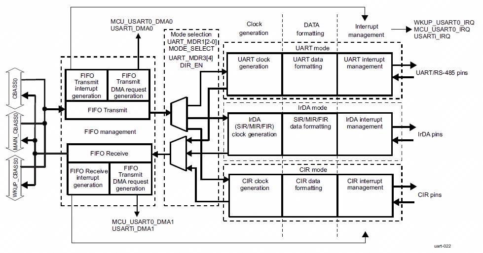
Figure 1-1 shows the Jacinto 7 UART functional block diagram. When the processor needs to send data, it only needs to write the output data into the FIFO through CPU/DMA. Then, the data is automatically transmitted to TX pin by UART_THR register and converted into TTL level. The data transmission is completed if the UART_THR register is empty. During the data receiving process, the TTL level is firstly converted into bit data through the pin, and is written to the FIFO by UART_RHR. When the FIFO reaches a threshold (maximum 64 Bytes), a CPU/DMA interrupt will be triggered to write the data to the memory. When enough data is read and the data in the FIFO is lower than the threshold, the interrupt condition disappears and the data receiving is finished.
 Figure 1-1 UART Functional Block
Diagram