SLVA505A February 2012 – July 2024 DRV8800 , DRV8801 , DRV8802 , DRV8803 , DRV8804 , DRV8805 , DRV8806 , DRV8811 , DRV8812 , DRV8813 , DRV8814 , DRV8818 , DRV8821 , DRV8823 , DRV8824 , DRV8828 , DRV8829 , DRV8830 , DRV8832 , DRV8832-Q1 , DRV8833 , DRV8834 , DRV8835 , DRV8836 , DRV8837 , DRV8840 , DRV8841 , DRV8842 , DRV8843 , DRV8844 , DRV8870 , DRV8871 , DRV8872
- 1
- Abstract
- Trademarks
- 1Factors Limiting the Maximum Output Current of a Motor Driver
- 2TI Motor Driver OCP Operation
- 3TI Motor Driver Data Sheet Ratings
- 4References
- 5Revision History
1.4.4 Thermal Vias
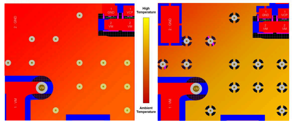
Thermal vias need to establish connections between the top and bottom layer to facilitate heat dissipation from the motor driver to the lower temperature PCB areas on the outer or inner PCB layers while the landing pad/thermal pad interface is dissipating heat on the top layer (device layer). Avoid thermal relief connections as they restrict heat flow, causing increased temperatures around vias. Directly connecting vias minimizes thermal resistance between the via and copper layers. When connecting thermal vias to the internal ground plane, make sure a complete connection around the entire circumference of the plated through hole. Avoid covering the vias with solder mask to prevent excessive voiding. Properly implementing thermal vias can assist with heat dissipation and help with more effective PCB performance and motor driver current ratings.
Though the thermal pad establishes a low-impedance thermal pathway between the die and the top ground plane of the PCB, it’s important to assess the thermal impedance of the vias connecting the top and bottom ground planes. The suggestion is to use thermal vias directly beneath the thermal pad, sized at 20 mil in diameter with a hole size of 8 mil which can keep the thermal resistance of the via to a minimum by minimizing solder wicking from the thermal pad.
 Figure 1-4 Thermal Relief vs
Direct-Connect Heat Map