SLYA091 December 2024 ISO5451 , ISO5452 , ISO5851 , ISO5852S , ISO5852S-EP , UCC21710 , UCC21710-Q1 , UCC21732 , UCC21732-Q1 , UCC21737-Q1 , UCC21739-Q1 , UCC21750 , UCC21750-Q1 , UCC21755-Q1 , UCC21756-Q1 , UCC21759-Q1 , UCC5310 , UCC5350 , UCC5350-Q1
Introduction
Gate drivers integrate active protection features to help reduce external circuitry, for example, an active Miller clamp. So how do designers determine if a design requires a Miller clamp? Understanding the sources of parasitics within switching applications and choosing a unipolar or bipolar power supply can help engineers make this decision. This application brief explores the design factors that influence the need for a Miller clamp, the trade-offs of implementing the clamp internally versus externally, and provides an example application where a Miller clamp is needed. The application brief also provides clear evaluation criterion for engineers deciding if a Miller clamp is necessary for their designs. This article is targeted at power electronic engineers who are designing high-speed switching applications.Understanding the Threat Posed by Parasitics
Every MOSFET and IGBT possesses parasitic capacitance. Using the following model from TI’s Fundamentals of MOSFET and IGBT Gate Driver Circuits application note (Figure 1), engineers can understand where this parasitic capacitance comes from.
 Figure 1 Power MOSFET Module
CGS and CGD are related to the geometry of the MOSFET and IGBT while CDS is the capacitance of the base-collector diode of the parasitic body diode. CGS is the gate-to-source capacitance, due to the overlap of the gate with the source region and the intrinsic capacitance between the gate and source terminals. CGD is the gate-to-drain capacitance, which is also known as the Miller Capacitance. CISS is the sum of the gate-to-source capacitance and the gate-to-drain capacitance, shown by the following equation.
CISS is a critical parameter for determining how fast the MOSFET or IGBT can switch and how much power is required to drive the transistor. CGD, along with a high dV/dt, pushes the charge into the gate which can cause a false turn-on.
PCB traces are the greatest source of parasitic inductance. A longer PCB trace results in greater parasitic inductance since inductance increases with conductor length. These parasitics combine to form the following resonant circuit in the gate-drive system:
 Figure 2 Gate Drive Resonant Circuit Components
At the moment of power, switches turn-off and dV/dt can be forced across the power switch; driven by the resonant circuit of parasitic components. This relationship is shown in Equation 2.
The dV/dt coupling with CGD (the parasitic capacitance) induces the Miller current. The increased temperature from operation causes the threshold voltage of the power switch to lower, and the induced Miller current can combine with the parasitic inductance to cause accidental charging and turn-on of the power switch. In a half-bridge circuit, as one MOSFET switches off and the other turns on, the rapid dV/dt across the off drain of the MOSFET induces a current through the Miller capacitance, charging the gate. This Miller current can raise the gate voltage higher, toward or above the threshold, causing an unintended turn-on of the switch that is to be off. This accidental turn-on can lead to a shoot-through event, where both power switches are conducting. A shoot-through event can lead to destruction of the power stage of the circuit and complete system failure.
Throughout the design process, considering the parasitic capacitance of the power switch is crucial. According to the manufacturer's data sheet, FET manufacturers do not typically list parasitic capacitance specifications which align with our CGS and CGD terms. Using the relevant equations for deriving these terms is important and can be found in, Fundamentals of MOSFET and IGBT Gate Driver Circuits application note. Additionally, following the layout recommendations of the component and minimizing PCB traces helps reduce the effects of the resonant circuit.
Unipolar Versus Bipolar Supply
Another important design factor in deciding if a Miller clamp is required for an application is the presence of a unipolar or bipolar power supply. As discussed, the Miller current is most likely to induce and cause an accidental turn-on of the power switch during a power switch turn-off event. If the design is using a unipolar power supply, with the negative rail of the gate driver connected to ground at 0V, this means the induced current only needs to cause a voltage spike from 0V to the threshold voltage of the power switch. Using a bipolar power supply allows the negative rail of the gate driver to connect to a hypothetical voltage of -8V. Now, the dV/dt conditions need to cause a voltage spike from -8V to the threshold voltage of the power switch. Using a bipolar power supply in a design can help completely remove the need for a Miller clamp while still providing protection against shoot-through conditions. Using a bipolar power supply requires an additional isolated bias function, which increases the system cost and requires additional PCB space. Design engineers must weigh this trade-off when considering whether to use a unipolar or bipolar power supply. When comparing the design consequences of a unipolar versus bipolar power supply, TI recommends implementing a Miller clamp for a unipolar power supply to offset the small voltage spike necessary for accidental turn-on of the power switch.
The High-Frequency Nature of the Miller Charge Injection
Due to the high-frequency nature of the Miller charge injection, the inductance of the VGS turn-off loop affects how much the voltage rises, which can then lead to unintentional turn-on of the transistor. As the frequency increases, the inductance presents a higher impedance to the current flow, resulting in higher voltages.
 Figure 3 Effect of the
High Frequency Miller Charge Injection on Voltage
Level
Figure 3 Effect of the
High Frequency Miller Charge Injection on Voltage
LevelPurpose of the Miller Clamp and Internal Versus External Implementation
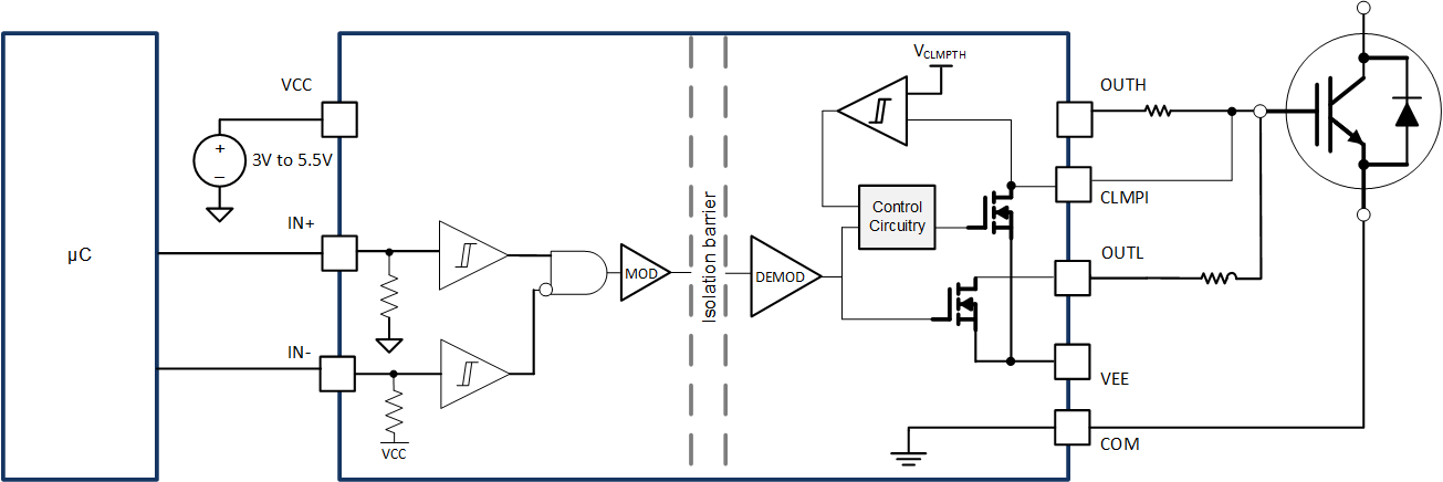
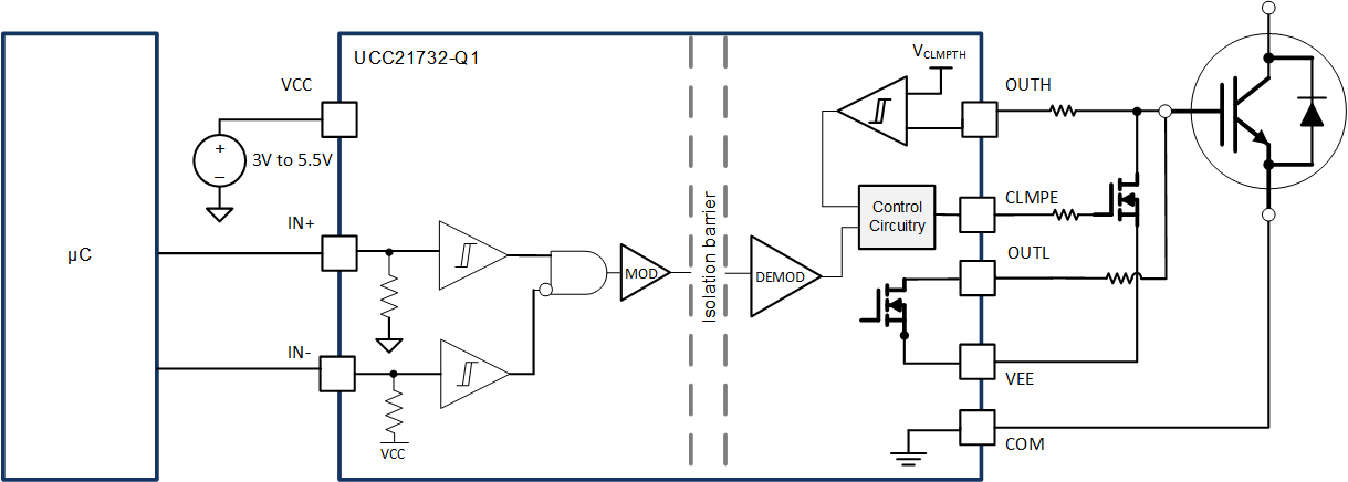
Increasing gate resistance is one method to slow or control the dV/dt and limit the Miller current, but this increase leads to an increase in power losses and reduced system efficiency. Using a Miller clamp in the design provides an alternate, low-impedance path for the Miller current to travel through without increasing power losses in the system. The UCC217xx/-Q1 isolated gate driver family offers both internal (CLMPI) and external (CLMPE) Miller clamp options (Figure 4 and Figure 5).
 Figure 4 Internal Active Miller Clamp in UCC21710
 Figure 5 External Miller Clamp in UCC21732
To effectively direct the Miller current to the negative supply voltage (denoted as VEE), the Miller clamp connection pin must be placed as close to the power module gate as possible, reducing the trace inductance between the gate and the Miller clamp FET. The functionality of an internal Miller clamp reduces the amount of external circuitry and PCB space for a lower system cost, overall. A CLMPE must be used if routing the CLMPI pin to a power module gate with a short trace is not possible.
When driving parallel FETs, a CLMPE is a better option than a CLMPI because of longer traces and, therefore, higher parasitics. CLPME can be placed close to individual gates, minimizing the impedance to negative bias. External implementation of the Miller clamp provides customers with more flexibility on the parameters of the Miller clamp. Key parameters include the clamp threshold voltage and Miller clamp pulldown drive strength. The clamp threshold voltage is predetermined by the gate driver specifications.
Application Example
Based on the information and design considerations explored, an evaluation criterion can be formed for when a design requires a Miller clamp. Imagine an example circuit using a unipolar power supply and a MOSFET with a 4V maximum gate threshold. Engineers must analyze the worst-case dV/dt conditions expected in the circuit. For this application example, a 50V change in 1ns is considered. Using the data sheet of the FET, the Miller capacitance can be approximated from the VDS versus capacitance curve following the CRSS value. Data sheet specifications in a table are not always applicable for the operating conditions of an application. Therefore, always follow the curve based on the worst-case conditions expected at FET turn-off. In this example, CRSS 20pF is used. Plugging these values into Equation 3, yields Equation 4.
Following Ohm’s Law and using a gate resistance value of 5Ω, this example results in a 5V spike on the power MOSFET. Since the MOSFET has a maximum gate threshold of 4V, this value leads to an accidental turn-on of the power switch and potentially a shoot-through event resulting in system failure.
As mentioned, a Miller clamp provides a low-impedance path for the Miller current to travel through. UCC5350MCDR offers an integrated Miller clamp with 0.26Ω clamp resistance. In the same application example, this value results in a 0.26V spike on the gate of the MOSFET and an accidental turn-on is avoided.
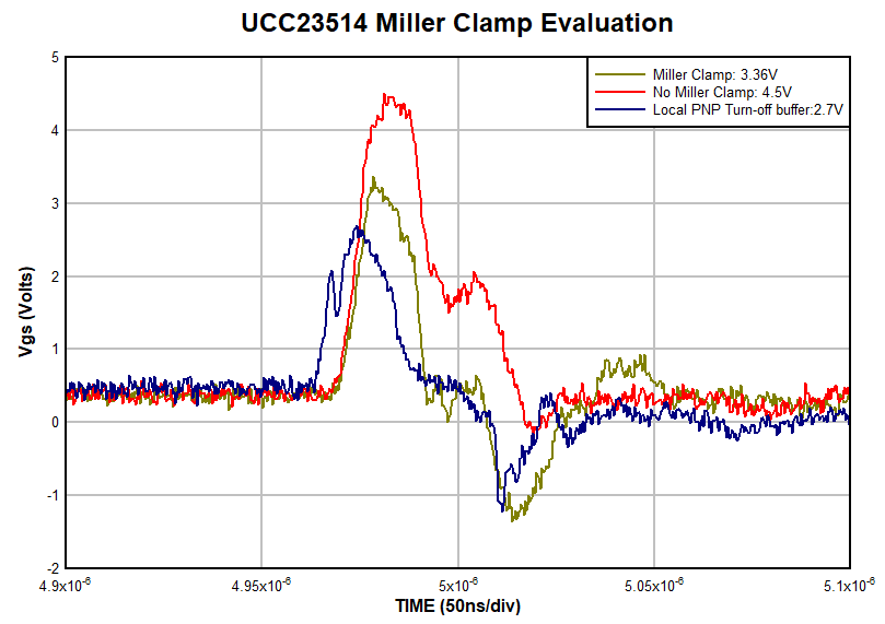
Figure 6 shows the comparison in UCC23514MDWVR VGS peak values between using a Miller clamp and not using a Miller clamp. The peak VGS value, with and without a Miller clamp respectively, is 3.36V and 4.5V. The use of a Miller clamp reduced the peak VGS value by 1.14V.
 Figure 6 UCC23514 Miller Clamp Evaluation
Devices With Internal and External Miller Clamp Options
Texas Instruments has many isolated gate driver families and device variants with an internal Miller clamp, and the UCC5350MCDR is a great example of a high-performing gate driver.
However, variants of the UCC21732 offer both internal and external Miller clamp options.
| Device OPN | CLMPI or CLMPE |
|---|---|
| UCC5350MCDR | CLMPI |
| ISO5451DWR | CLMPI |
| UCC21732QDWRQ1 | CLMPE |
| UCC21710DWR | CLMPI |
Conclusion
Deciding to incorporate a Miller clamp into a design depends on system parasitics, the type of power supply used, and the high-frequency nature of the Miller injection. Miller clamps are integral for avoiding unintentional turn-on of the FET, which can cause unpredictable behavior and damage to the device. Designs involving fast switching transistors, requiring precise control over voltage changes, requires a Miller clamp to improve the robustness and reliability of the system. Ultimately, careful analysis of the behavior of the circuit under high-frequency conditions provides insight into determining the necessity and value of adding a Miller clamp to the design.