SNOAA35F April 2019 – December 2024 LM2901 , LM2901B , LM2901B-Q1 , LM2903 , LM2903-Q1 , LM2903B , LM2903B-Q1 , LM339 , LM339-N , LM393 , LM393-N , LM393B , LM397 , TL331 , TL331-Q1 , TL331B
- 1
- Abstract
- Trademarks
- 1 Devices Covered in Application Note
- 2 The New TL331B, TL391B, LM339B, LM393B, LM2901B and LM2903B B Versions
- 3 PCN's to Change Classic Die to a New Die Design
- 4 Changes to Package Top Markings
- 5 Roughened Leadframe Finish
-
6 Input Considerations
- 6.1 Input Stage Schematic – The Classic LM339 Family
- 6.2 Input Stage Schematic - New "B" and TiB Devices
- 6.3 Differences Between the Classic, "B" and Tib Die Devices
- 6.4 Input Voltage Range
- 6.5 Input Voltage Range vs. Common Mode Voltage Range
- 6.6 Reason for Input Range Headroom Limitation
- 6.7 Input Voltage Range Feature
- 6.8 Both Inputs Above Input Range Behavior
- 6.9 Negative Input Voltages
- 6.10 Power-Up Behavior
- 6.11 Capacitors and Hysteresis
- 6.12 Output to Input Cross-Talk
- 7 Output Stage Considerations
- 8 Power Supply Considerations
- 9 General Comparator Usage
- 10PSpice and TINA TI Models
- 11Conclusion
- 12Related Documentation
- 13Revision History
6.9.3.2.1 Split Voltage Divider with Clamp
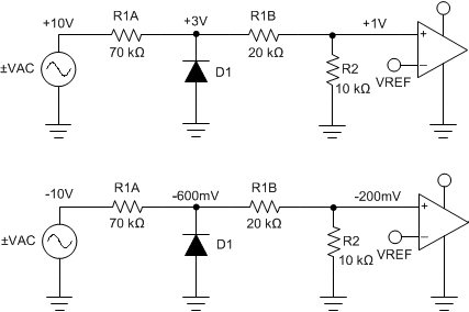
To improve upon the voltage divider described above, the upper voltage divider resistor can be split and apply the clamp diode at the higher tap voltage, as shown in Figure 6-9. The idea is that two bottom resistors (R1B and R2) further divide down the diode clamped voltage to bring the clamped voltage to a safe level at the input.
 Figure 6-9 Split Voltage Divider Negative Voltage Protection
The upper common voltage divider resistor R1 is split into two resistors, R1A and R1B, providing a higher voltage tap sample point for the clamp diode. The clamp diode maintains that the tap voltage does not exceed -600mV as the input voltage moves further negative.
With a positive input voltage, the diode is reverse biased and does not conduct, effectively removing the diode from the circuit (except for some small leakage current). The voltage divider R1A + R1B combine create the upper R1 voltage divider resistor against R2.
When the input voltage is negative, the diode clamps the node between R1A and R1B to -600mV. R1B and R2 then create a 3x voltage divider, which results in a safer -200mV on the input. Note that R1A now has the full input voltage across the resistor and needs to be sized appropriately.
The design procedure is fairly simple. The full divider is calculated as a normal two resistor voltage divider, deriving the needed R1 and R2 values. The desired secondary negative R1B divider is then calculated from the existing R2 and required portion of R1.