SNOAA35F April 2019 – December 2024 LM2901 , LM2901B , LM2901B-Q1 , LM2903 , LM2903-Q1 , LM2903B , LM2903B-Q1 , LM339 , LM339-N , LM393 , LM393-N , LM393B , LM397 , TL331 , TL331-Q1 , TL331B
- 1
- Abstract
- Trademarks
- 1 Devices Covered in Application Note
- 2 The New TL331B, TL391B, LM339B, LM393B, LM2901B and LM2903B B Versions
- 3 PCN's to Change Classic Die to a New Die Design
- 4 Changes to Package Top Markings
- 5 Roughened Leadframe Finish
-
6 Input Considerations
- 6.1 Input Stage Schematic – The Classic LM339 Family
- 6.2 Input Stage Schematic - New "B" and TiB Devices
- 6.3 Differences Between the Classic, "B" and Tib Die Devices
- 6.4 Input Voltage Range
- 6.5 Input Voltage Range vs. Common Mode Voltage Range
- 6.6 Reason for Input Range Headroom Limitation
- 6.7 Input Voltage Range Feature
- 6.8 Both Inputs Above Input Range Behavior
- 6.9 Negative Input Voltages
- 6.10 Power-Up Behavior
- 6.11 Capacitors and Hysteresis
- 6.12 Output to Input Cross-Talk
- 7 Output Stage Considerations
- 8 Power Supply Considerations
- 9 General Comparator Usage
- 10PSpice and TINA TI Models
- 11Conclusion
- 12Related Documentation
- 13Revision History
6.6 Reason for Input Range Headroom Limitation
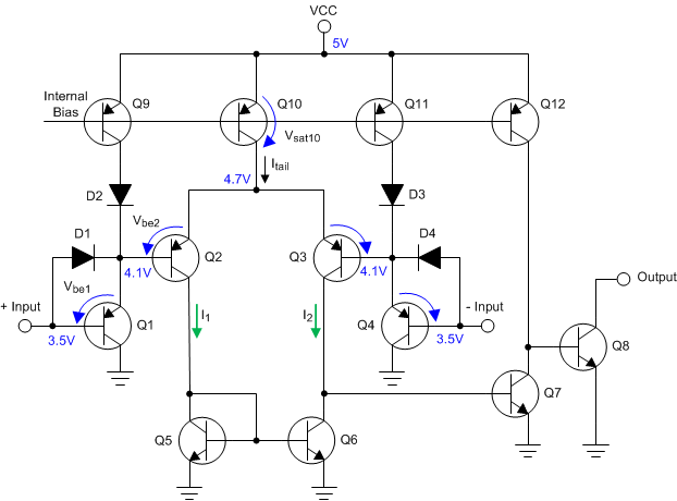
The LM339 family was the first truly single-supply, ground sensing comparator, but is not a Rail-to-Rail input device and can only sense up to about 1.5V below VCC. The input stage requires some headroom to the VCC supply to provide the needed tail current and biasing to the input devices Q1 through Q4. Assuming a 5V supply, Figure 6-4 shows the necessary voltage drops from the supply voltage down to the input terminal.
 Figure 6-4 Headroom Taken Up by VBE's and VSAT of Input Stage
The DC biasing current flows down from VCC , through the Q10 current source, through the input pair Q2 and Q1, and out of the input pin towards ground through the input source resistance.
The required headroom can be analyzed by Counting VBE's, starting at the VCC rail and down to the input pin. Starting at VCC, about 250-300mV is dropped across the current source Q10 collector-emitter junction (VSAT10). Another 600mV is dropped across each of the Base-Emitter junctions of Q2 (VBE2) and Q1 (VBE1). By adding all the drops together (VSAT10 + VBE1 + VBE2 ), there needs to be at least a 1.5V headroom between the input pin and VCC for the input stage to bias properly.
If an input is brought above the input limit, that input transistor starts to turn off, and the tail current for that device (I1 or I2) is also cut off.
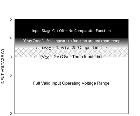
 Figure 6-5 Visual Representation of Input Voltage Range With a 5V Supply
Figure 6-5 shows a visual representation of the input voltage range with a single +5 V supply.
Between 0V and 3V (VCC - 2V), the device is fully operational and functions per the data sheet specifications over the full specified temperature range. The VCC - 2V limit is the recommended upper input range limit to be utilized for all designs.
The input range from 0 to 3.5V (VCC - 1.5V) is valid at 25°C and above. The range between 3V and 3.5V can vary over temperature due to the VBE's of the transistors changing at -2.1mV/°C. This results in the input voltage range changing at -4.2mV/°C over temperature (note the negative sign!), necessitating the VCC - 2V over temperature specification. Using the VCC - 1.5V limit can cause The design worked fine on the bench, but fails at cold complaints. Do not make this mistake!
The range between 3.5V and 4V is the gray zone, where the device appears to still function at 25°C and above, but critical specifications are deteriorating, such as offset voltage, bias current and particularly propagation delay as the input stage is gradually starved. These effects are not be immediately apparent. Operating at low temperatures can cause failures. Operation within this zone must be avoided.
Between 4V and 5V, and even up to 36V, the input stage is cut off and input bias current falls to near zero. The actual cut-off threshold depends on temperature. Comparator operation ceases. DO NOT operate in this area!