SNOAA35F April 2019 – December 2024 LM2901 , LM2901B , LM2901B-Q1 , LM2903 , LM2903-Q1 , LM2903B , LM2903B-Q1 , LM339 , LM339-N , LM393 , LM393-N , LM393B , LM397 , TL331 , TL331-Q1 , TL331B
- 1
- Abstract
- Trademarks
- 1 Devices Covered in Application Note
- 2 The New TL331B, TL391B, LM339B, LM393B, LM2901B and LM2903B B Versions
- 3 PCN's to Change Classic Die to a New Die Design
- 4 Changes to Package Top Markings
- 5 Roughened Leadframe Finish
-
6 Input Considerations
- 6.1 Input Stage Schematic – The Classic LM339 Family
- 6.2 Input Stage Schematic - New "B" and TiB Devices
- 6.3 Differences Between the Classic, "B" and Tib Die Devices
- 6.4 Input Voltage Range
- 6.5 Input Voltage Range vs. Common Mode Voltage Range
- 6.6 Reason for Input Range Headroom Limitation
- 6.7 Input Voltage Range Feature
- 6.8 Both Inputs Above Input Range Behavior
- 6.9 Negative Input Voltages
- 6.10 Power-Up Behavior
- 6.11 Capacitors and Hysteresis
- 6.12 Output to Input Cross-Talk
- 7 Output Stage Considerations
- 8 Power Supply Considerations
- 9 General Comparator Usage
- 10PSpice and TINA TI Models
- 11Conclusion
- 12Related Documentation
- 13Revision History
6.1 Input Stage Schematic – The Classic LM339 Family
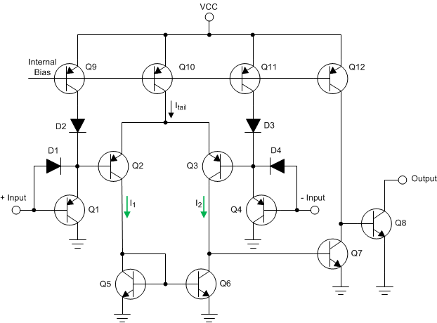
The simplified classic LM339 Family comparator internal schematic is shown in Figure 6-1. Minus a few devices in the biasing circuitry, the schematic is a fairly true representation of the actual internal circuit.
The input stage consists of the PNP Darlington Input Pairs Q1+Q2, and Q3+Q4, the bias mirror Q10 to provide the operating tail currents, and the active load of Q5 and Q6. The output stage is comprised of Q7, Q12 and output transistor Q8. Diodes D1 through D4 protect the input devices when the inputs are taken above V+.
 Figure 6-1 Simplified Input Stage Schematic with All Current Source Connections
The schematic also contains additional current source lines (Q9, D2, Q11, and D3) not drawn in the simplified schematic found in the data sheets. All PNP emitters in the Darlington input stage have current source connections. These current sources maintain a consistent input bias current that does not vary with the differential input voltage. This consistent current provides a high effective input to input resistance. Without these secondary current sources, the input bias current can vary from zero to twice the normal bias current as the differential input voltage is varied.