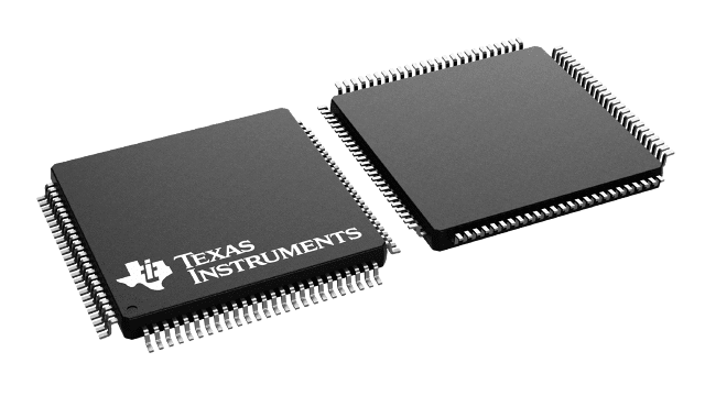
Gehäuseinformationen
| Gehäuse | Pins LQFP (PZ) | 100 |
| Betriebstemperaturbereich (°C) -55 to 125 |
| Gehäusemenge | Träger 90 | JEDEC TRAY (5+1) |
Merkmale von SM320F2801-EP
- Controlled Baseline
- One Assembly/Test/Fabrication Site
- Enhanced Diminishing Manufacturing Sources (DMS) Support
- Enhanced Product-Change Notification
- Qualification Pedigree(1)
- High-Performance Static CMOS Technology
- 100 MHz (10-ns Cycle Time)
- Low-Power (1.8-V Core, 3.3-V I/O) Design
- 3.3-V Flash Voltage
- JTAG Boundary Scan Support
- High-Performance 32-Bit CPU (TMS320C28x)
- 16 x 16 and 32 x 32 MAC Operations
- 16 x 16 Dual MAC
- Harvard Bus Architecture
- Atomic Operations
- Fast Interrupt Response and Processing
- Unified Memory Programming Model
- Code-Efficient (in C/C++ and Assembly)
- On-Chip Memory
- F2808: 64K X 16 Flash, 18K X 16 SARAM
F2806: 32K X 16 Flash, 10K X 16 SARAM
F2801: 16K X 16 Flash, 6K X 16 SARAM
9501: 16K X 16 Flash, 6K X 16 SARAM - 1K x 16 OTP ROM
- F2808: 64K X 16 Flash, 18K X 16 SARAM
- Boot ROM (4K x 16)
- With Software Boot Modes (via SCI, SPI, CAN, I2C, and Parallel I/O)
- Standard Math Tables
- Clock and System Control
- Dynamic PLL Ratio Changes Supported
- On-Chip Oscillator
- Clock-Fail-Detect Mode
- Watchdog Timer Module
- Any GPIO A Pin Can Be Connected to One of the Three External Core Interrupts
- Peripheral Interrupt Expansion (PIE) Block That Supports All 43 Peripheral Interrupts
- 128-Bit Security Key/Lock
- Protects Flash/OTP/L0/L1 Blocks
- Prevents Firmware Reverse Engineering
- Enhanced Control Peripherals
- Up to 16 PWM Outputs
- Up to Four HRPWM Outputs With 150 ps MEP Resolution
- Up to Four Capture Inputs
- Up to Two Quadrature Encoder Interfaces
- Up to Six 32-bit Timers
- Up to Six 16-bit Timers
- Three 32-Bit CPU Timers
- Serial Port Peripherals
- Up to Four Serial Peripheral Interface (SPI) Modules
- Up to Two Serial Communications Interface (SCI), Standard UART Modules
- Up to Two Enhanced Controller Area Network (eCAN) Modules
- One Inter-Integrated-Circuit (I2C) Bus
- 12-Bit ADC, 16 Channels
- 2 x 8 Channel Input Multiplexer
- Two Sample-and-Hold
- Single/Simultaneous Conversions
- Fast Conversion Rate: 160 ns/6.25 MSPS
- Internal or External Reference
- Up to 35 Individually Programmable, Multiplexed General-Purpose Input/Output (GPIO) Pins With Input Filtering
- Advanced Emulation Features
- Analysis and Breakpoint Functions
- Real-Time Debug via Hardware
- Low-Power Modes and Power Savings
- IDLE, STANDBY, HALT Modes Supported
- Disable Individual Peripheral Clocks
- Package Options
- Thin Quad Flatpack (PZ)
- MicroStar BGA™ (GGM, ZGM)
- Temperature Options:
- M: -55°C to 125°C (PZ)
(1) Component qualification in accordance with JEDEC and industry standards to ensure reliable operation over an extended temperature range. This includes, but is not limited to, Highly Accelerated Stress Test (HAST) or biased 85/85, temperature cycle, autoclave or unbiased HAST, electromigration, bond intermetallic life, and mold compound life. Such qualification testing should not be viewed as justifying use of this component beyond specified performance and environmental limits.
MicroStar BGA, TMS320C28x, MicroStar, C28x, TMS320C2000, DSP/BIOS, Code Composer Studio, TMS320 are trademarks of Texas Instruments.
eZdsp, XDS510USB are trademarks of Spectrum Digital.
Beschreibung von SM320F2801-EP
The SM320F2808, F2806, and F2801/UCD9501 devices, members of the TMS320C28x™ DSP generation, are highly integrated, high-performance solutions for demanding control applications. The UCD9501 is a 32-bit digital signal controller for power management.
Throughout this document, SM320F2808, F2806, and F2801/UCD9501 are abbreviated as F2808, F2806, and F2801/9501, respectively. TMS320x280x device reference guides, flash tools, and other collateral are applicable to the UCD9501 device as well.
