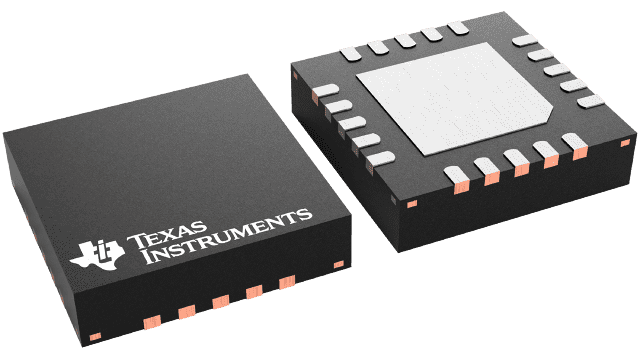
パッケージ情報
| パッケージ | ピン数 VQFN (RGP) | 20 |
| 動作温度範囲 (℃) -40 to 85 |
| パッケージ数量 | キャリア 92 | TUBE |
CC1101 の特徴
- RF Performance
- High sensitivity
- –116 dBm at 0.6 kBaud, 433 MHz, 1% packet error rate
- –112 dBm at 1.2 kBaud, 868 MHz, 1% packet error rate
- Low current consumption (14.7 mA in RX, 1.2 kBaud, 868 MHz)
- Programmable output power up to +12 dBm for all supported frequencies
- Excellent receiver selectivity and blocking performance
- Programmable data rate from 0.6 to 600 kbps
- Frequency bands: 300-348 MHz, 387-464 MHz and 779-928 MHz
- High sensitivity
- Analog Features
- 2-FSK, 4-FSK, GFSK, and MSK supported as well as OOK
and flexible ASK shaping - Suitable for frequency hopping systems due to a fast settling
frequency synthesizer; 75 µs settling time - Automatic Frequency Compensation (AFC) can be used to align the frequency
synthesizer to the received signal centre frequency - Integrated analog temperature sensor
- 2-FSK, 4-FSK, GFSK, and MSK supported as well as OOK
- Digital Features
- Flexible support for packet oriented systems; On-chip support for
sync word detection, address check, flexible packet length, and
automatic CRC handling - Efficient SPI interface; All registers can be programmed with
one "burst" transfer - Digital RSSI output
- Programmable channel filter bandwidth
- Programmable Carrier Sense (CS) indicator
- Programmable Preamble Quality Indicator (PQI) for improved protection
against false sync word detection in random noise - Support for automatic Clear Channel Assessment (CCA) before transmitting
(for listen-before-talk systems) - Support for per-package Link Quality Indication (LQI)
- Optional automatic whitening and de-whitening of data
- Flexible support for packet oriented systems; On-chip support for
- Low-Power Features
- 200 nA sleep mode current consumption
- Fast startup time; 240 µs from sleep to RX or TX
mode (measured on EM reference design [1] and [2]) - Wake-on-radio functionality for automatic low-power RX polling
- Separate 64-byte RX and TX data FIFOs (enables burst mode data transmission)
- General
- Few external components; Completely on-chip frequency synthesizer, no external
filters or RF switch needed - Green package: RoHS compliant and no antimony or bromine
- Small size (QLP 4x4 mm package, 20 pins)
- Suited for systems targeting compliance with EN 300 220 (Europe) and
FCC CFR Part 15 (US) - Suited for systems targeting compliance with the Wireless MBUS standard EN 13757-4:2005
- Support for asynchronous and synchronous serial receive/transmit mode for backwards
compatibility with existing radio communication protocols
- Few external components; Completely on-chip frequency synthesizer, no external
- Improved Range using CC1190
- The CC1190 [21] is a range extender for 850-950 MHz and is an ideal
fit for CC1101 to enhance RF performance - High sensitivity–118 dBm at 1.2 kBaud, 868 MHz, 1% packet error
rate–120 dBm at 1.2 kBaud, 915 MHz, 1% packet error rate - +20 dBm output power at 868 MHz
- +27 dBm output power at 915 MHz
- Refer to AN094 [22] and AN096 [23] for more performance figures of the
CC1101 + CC1190 combination
- The CC1190 [21] is a range extender for 850-950 MHz and is an ideal
- Reduced Battery Current using TPS62730
- The TPS62730 [26] is a step down converter with bypass mode for
ultra low power wireless applications - In RX, the current drawn from a 3.6 V battery is typically less than
11 mA when TPS62730 output voltage is 2.1 V. When connecting CC1101
directly to a 3.6 V battery the current drawn is typically 17 mA - In TX, at maximum output power (+12 dBm), the current drawn from a
3.6 V battery is typically 22 mA when TPS62730 output voltage is 2.1 V.
When connecting CC1101 directly to a 3.6 V battery the current drawn is
typically 34 mA - When CC1101 enters SLEEP mode, the TPS62730 can be put
in bypass mode for very low power down current - The typical TPS62730 current consumption is 30 nA in bypass mode.
- The CC1101 is connected to the battery via an integrated 2.1 Ω (typical)
switch in bypass mode
- The TPS62730 [26] is a step down converter with bypass mode for
CC1101 に関する概要
CC1101 is a low-cost sub-1 GHz transceiver designed for very low-power wireless applications. The circuit is mainly intended for the ISM (Industrial, Scientific and Medical) and SRD (Short Range Device) frequency bands at 315, 433, 868, and 915 MHz, but can easily be programmed for operation at other frequencies in the 300-348 MHz, 387-464 MHz and 779-928 MHz bands.
The RF transceiver is integrated with a highly configurable baseband modem. The modem supports various modulation formats and has a configurable data rate up to 600 kbps.
CC1101 provides extensive hardware support for packet handling, data buffering, burst transmissions, clear channel assessment, link quality indication, and wake-on-radio.
The main operating parameters and the 64- byte transmit/receive FIFOs of CC1101 can be controlled via an SPI interface. In a typical system, the CC1101 will be used together with a microcontroller and a few additional passive components.
The CC1190 850-950 MHz range extender [21] can be used with CC1101 in long range applications for improved sensitivity and higher output power.
