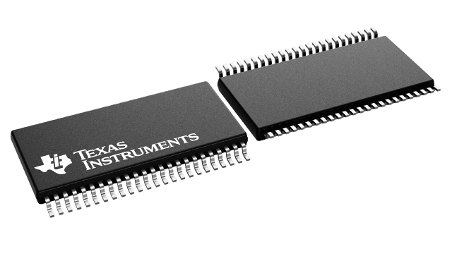
パッケージ情報
| パッケージ | ピン数 TSSOP (DGG) | 48 |
| 動作温度範囲 (℃) |
| パッケージ数量 | キャリア 40 | TUBE |
SN74ALVC164245 の特徴
- Member of the Texas Instruments Widebus™ Family
- Maximum tpd of 5.8 ns at 3.3 V
- ±24-mA Output Drive at 3.3 V
- Control Inputs VIH/VIL Levels Are Referenced to VCCA Voltage
- Latch-Up Performance Exceeds 250 mA Per JESD 17
- APPLICATIONS
- Electronic Points of Sale
- Printers and Other Peripherals
- Motor Drives
- Wireless and Telecom Infrastructures
- Wearable Health and Fitness Devices
All other trademarks are the property of their respective owners
SN74ALVC164245 に関する概要
This 16-bit (dual-octal) noninverting bus transceiver contains two separate supply rails. B port has VCCB, which is set to operate at 3.3 V and 5 V. A port has VCCA, which is set to operate at 2.5 V and 3.3 V. This allows for translation from a 2.5-V to a 3.3-V environment, and vice versa, or from a 3.3-V to a 5-V environment, and vice versa.
The SN74ALVC164245 is designed for asynchronous communication between data buses. The control circuitry (1DIR, 2DIR, 1OE, and 2OE) is powered by VCCA.
To ensure the high-impedance state during power up or power down, the output-enable (OE) input should be tied to VCC through a pullup resistor; the minimum value of the resistor is determined by the current-sinking capability of the driver.
The logic levels of the direction-control (DIR) input and the output-enable (OE) input activate either the B-port outputs or the A-port outputs or place both output ports into the high-impedance mode. The device transmits data from the A bus to the B bus when the B-port outputs are activated, and from the B bus to the A bus when the A-port outputs are activated. The input circuitry on both A and B ports always is active and must have a logic HIGH or LOW level applied to prevent excess ICC and ICCZ.
