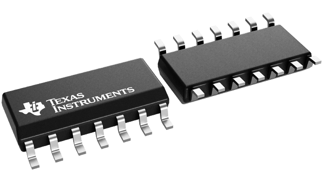
封裝資訊
| 封裝 | 針腳 SOIC (D) | 14 |
| 操作溫度範圍 (°C) -55 to 125 |
| 包裝數量 | 運送業者 250 | SMALL T&R |
CD74HC107 的特色
- Hysteresis on Clock Inputs for Improved Noise Immunity and Increased Input Rise and Fall Times
- Asynchronous Reset
- Complementary Outputs
- Buffered Inputs
- Typical fMAX = 60MHz at VCC = 5V, CL = 15pF, TA = 25°C
- Fanout (Over Temperature Range)
- Standard Outputs . . . . . . . . . . . . . . . 10 LSTTL Loads
- Bus Driver Outputs . . . . . . . . . . . . . 15 LSTTL Loads
- Wide Operating Temperature Range . . . -55°C to 125°C
- Balanced Propagation Delay and Transition Times
- Significant Power Reduction Compared to LSTTL Logic ICs
- HC Types
- 2V to 6V Operation
- High Noise Immunity: NIL = 30%, NIH = 30% of VCC at VCC = 5V
- HCT Types
- 4.5V to 5.5V Operation
- Direct LSTTL Input Logic Compatibility, VIL = 0.8V (Max), VIH = 2V (Min)
- CMOS Input Compatibility, Il
 1µA at VOL, VOH
CD74HC107 的說明
The ’HC107 and ’HCT107 utilize silicon gate CMOS technology to achieve operating speeds equivalent to LSTTL parts. They exhibit the low power consumption of standard CMOS integrated circuits, together with the ability to drive 10 LSTTL loads.
These flip-flops have independent J, K, Reset and Clock inputs and Q and Q\ outputs. They change state on the negative-going transition of the clock pulse. Reset is accomplished asynchronously by a low level input.
This device is functionally identical to the HC/HCT73 but differs in terminal assignment and in some parametric limits.
The HCT logic family is functionally as well as pin compatible with the standard LS family.
