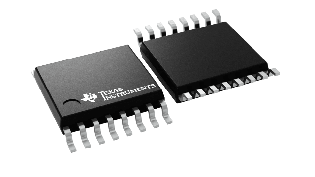
封裝資訊
| 封裝 | 針腳 TSSOP (PW) | 16 |
| 操作溫度範圍 (°C) -40 to 85 |
| 包裝數量 | 運送業者 2,500 | LARGE T&R |
LMK00804B 的特色
- Four LVCMOS/LVTTL Outputs with 7 Ω Output
Impedance- Additive Jitter: 0.04 ps RMS (typ) @ 125 MHz
- Noise Floor: –166 dBc/Hz (typ) @ 125 MHz
- Output Frequency: 350 MHz (max)
- Output Skew: 35 ps (max)
- Part-to-Part Skew: 700 ps (max)
- Two Selectable Inputs
- CLK, nCLK Pair Accepts LVPECL, LVDS,
HCSL, SSTL, LVHSTL, or LVCMOS/LVTTL - LVCMOS_CLK Accepts LVCMOS/LVTTL
- CLK, nCLK Pair Accepts LVPECL, LVDS,
- Synchronous Clock Enable
- Core/Output Power Supplies:
- 3.3 V/3.3 V
- 3.3 V/2.5 V
- 3.3 V/1.8 V
- 3.3 V/1.5 V
- Package: 16-Lead TSSOP
- Industrial Temperature Range: –40ºC to +85ºC
LMK00804B 的說明
The LMK00804B is a low skew, high performance clock fanout buffer which can distribute up to four LVCMOS/LVTTL outputs (3.3-V, 2.5-V, 1.8-V, or 1.5-V levels) from one of two selectable inputs, which can accept differential or single-ended inputs. The clock enable input is synchronized internally to eliminate runt or glitch pulses on the outputs when the clock enable terminal is asserted or de-asserted. The outputs are held in logic low state when the clock is disabled. A separate output enable terminal controls whether the outputs are active state or high-impedance state. The low additive jitter and phase noise floor, and guaranteed output and part-to-part skew characteristics make the LMK00804B ideal for applications demanding high performance and repeatability.
See also Device Comparison Table for descriptions of CDCLVC1310 and LMK00725 parts.
