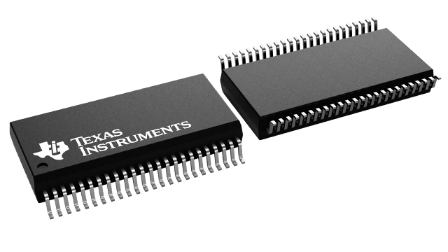
封裝資訊
| 封裝 | 針腳 SSOP (DL) | 48 |
| 操作溫度範圍 (°C) -40 to 85 |
| 包裝數量 | 運送業者 25 | TUBE |
SN74ALVTH162245 的特色
- State-of-the-Art Advanced BiCMOS Technology (ABT) Widebus™ Design for 2.5-V and 3.3-V Operation and Low Static-Power Dissipation
- Support Mixed-Mode Signal Operation (5-V Input and Output Voltages With 2.3-V to 3.6-V VCC)
- Typical VOLP (Output Ground Bounce)
<0.8 V at VCC = 3.3 V, TA = 25°C - High Drive
- A Port = –12/12 mA at 3.3-V VCC
- B port = –32/64 mA at 3.3-V VCC
- Ioff and Power-Up 3-State Support Hot Insertion
- Use Bus Hold on Data Inputs in Place of External Pullup/Pulldown Resistors to Prevent the Bus From Floating
- A-Port Outputs Have Equivalent 30-
 Series Resistors, So No External Resistors Are Required
 - Flow-Through Architecture Facilitates Printed Circuit Board Layout
- Distributed VCC and GND Pins Minimize High-Speed Switching Noise
- Latch-Up Performance Exceeds 100 mA Per JESD 78, Class II
Widebus is a trademark of Texas Instruments.
SN74ALVTH162245 的說明
The ’ALVTH162245 devices are 16-bit (dual-octal) noninverting 3-state transceivers designed for 2.5-V or 3.3-V VCC operation, but with the capability to provide a TTL interface to a 5-V system environment.
These devices can be used as two 8-bit transceivers or one 16-bit transceiver. They allow data transmission from the A bus to the B bus or from the B bus to the A bus, depending on the logic level at the direction-control (DIR) input. The output-enable (OE)\ input can be used to disable the device so that the buses are effectively isolated.
The A-port outputs, which are designed to source or sink up to 12 mA, include equivalent 30- series resistors to reduce overshoot and undershoot.
These devices are fully specified for hot-insertion applications using Ioff and power-up 3-state. The Ioff circuitry disables the outputs, preventing damaging current backflow through the device when it is powered down. The power-up 3-state circuitry places the outputs in the high-impedance state during power up and power down, which prevents driver conflict.
Active bus-hold circuitry is provided to hold unused or floating data inputs at a valid logic level. Use of pullup or pulldown resistors with the bus-hold circuitry is not recommended.
When VCC is between 0 and 1.2 V, the device is in the high-impedance state during power up or power down. However, to ensure the high-impedance state above 1.2 V, OE\ should be tied to VCC through a pullup resistor; the minimum value of the resistor is determined by the current-sinking capability of the driver.
