SLUAAW3 August 2024 TPSM82912 , TPSM82913 , TPSM82916 , TPSM843320 , TPSM843620 , TPSM843820 , TPSM843A22 , TPSM843A26 , TPSM843B22 , TPSM8D6B24 , TPSM8D6C24 , TPSM8S6C24
Due to the rapid development of artificial intelligence (AI), 5G, internet of things (IoT), and electric vehicles (EV), the demand for semiconductor testers and Automated Test Equipment (ATE) has been increasing in recent years. These industries feature increasingly complicated chips, and thus more powerful and precise ATE is needed to test them. When designing the power for semiconductor test equipment, the increasing complexity of these testers often results in increasing current requirements and a host of other special considerations.
When choosing DC/DC converters, there are often strict noise and frequency requirements involved to avoid affecting the measurement capabilities of the equipment. Similarly, many testers use high-powered FPGAs which often require low-ripple core rails. Above all else, semiconductor test equipment strives for maximum power density and for the smallest possible design size. This article describes common design challenges associated with using buck regulators for semiconductor testing and ATE power.
Table 1 lists DC/DC buck regulators recommended for semiconductor test and ATE power designs, including modules (integrated inductor) and converters (integrated FET, separate Inductor) which feature external frequency synchronization capabilities.
| Type | Module | VIN | IOUT | Size | Features | Converter |
|---|---|---|---|---|---|---|
| High Power Density | TPSM843320 | 4V–18V | 3A | 3.5mm × 3.5mm × 1.6mm | High efficiency, ACM, ±0.5% accuracy, Selectable FSW: 500kHz, 750kHz, 1MHz, 1.5MHz, 2.2MHz, FSYNC. Power good, Adj soft start. | TPS543320 |
| TPSM843620 | 4V–18V | 6A | TPS543620 | |||
| TPSM843820 | 4V–18V | 8A | TPS543820 | |||
| TPSM843A22 | 4V–18V | 12A | 6.5mm × 7.5mm × 4.0mm | High efficiency, ACM, ±0.5% accuracy, Selectable FSW: 500kHz, 750kHz, 1MHz, 1.5MHz, 2.2MHz, FSYNC. Power good, Adj soft start. | TPS543A22 | |
| TPSM843A26 | 4V–18V | 16A | TPS543A26 | |||
| TPSM843B22 | 4V–18V | 20A | TPS543B22 B25 |
|||
| Low Noise and Low Ripple | TPSM82912 | 3V–17V | 2A | 4.5mm × 5.5mm × 1.8mm | Eliminates low dropout (LDO) and passive post filtering, low noise and low ripple, CM, Spread spectrum modulation, FSW:1MHz, 2.2MHz, FSYNC. Power good, Adj soft start. | TPS62912 |
| TPSM82913 | 3V–17V | 3A | TPS62913 | |||
| TPSM82914 | 3V–17V | 4.5A | 4.0mm × 4.7mm × 2.9mm | Eliminates LDO and passive post filtering, low noise and low ripple, CM, Spread spectrum modulation, FSW:1MHz, 1.4MHz, 2.2MHz, FSYNC. Power good, Adj soft start. | TPS62914 | |
| TPSM82916 | 3V–17V | 6A | TPS62916, TPS62918 | |||
| PMBus® with Telemetry | TPSM8S6B24 | 4V–16V | 25A | 16mm × 11mm × 4.3mm | PMBus with telemetry, Stack x4, CM, FSW:275kHz to 1100kHz, FSYNC. Power good, Adj soft start. | TPS546B24S |
| TPSM8S6C24 | 4V–16V | 35A | TPS546D24S | |||
| TPSM8D6B24 | 4V–16V | 50A (Dual 25A) | 16mm × 20mm × 4.3mm | PMBus with telemetry, Stack x2, CM, FSW: 275kHz to 1100kHz, FSYNC. Power good, Adj soft start. | TPS546B24A | |
| TPSM8D6C24 | 4V–16V | 70A (Dual 35A) | TPS546D24A | |||
| 24V Input | TPSM84338 | 4.5V–28V | 3A | 3.3mm × 4.5mm × 2.0mm | Wide voltage range, CM, FSW: 200kHz to 2.2MHz, FSYNC, Spread spectrum modulation. Power good, Adj soft start. | TPS54538, TPS54338 |
Reducing Size With Module Designs
To simplify power design and minimize PCB size, use a buck module instead of a buck converter. Take TPSM843620 and the converter version TPS543620 as an example: the total size of the TPS543620 converter circuit design was measured to be approximately 100.8mm2, while the TPSM843620 module circuit design was measured to be only 66mm2, which is a 44% size reduction. Figure 1 illustrates the size reduction. Both the TPS543620 and TPSM843620 PCB design size were selected based on data sheet recommendations for identical applications.
 Figure 1 PCB Size Comparison Between
TPS543620 and TPSM843620
Figure 1 PCB Size Comparison Between
TPS543620 and TPSM843620Power Challenges
Power Density
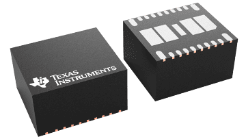
For ATE power design, board area and Z-height are generally the limiting factors as power demands increase. As a result of this, power modules are often chosen for point-of-load designs, as these modules allow for the smallest possible X-Y footprint. TI’s new TPSM843B22 buck module is one device that allows power designers to optimize designs for power density. The device provides 20A in a 6.5mm × 7.5mm package and includes a butterfly-style footprint. This footprint, when combined with the integrated inductor, allows for an optimized and symmetrical footprint of 212mm2 with an overmolded package that is only 4mm tall, as Figure 2 illustrates. Figure 3 shows the symmetrical nature of an example PCB layout for the device. With this symmetrical design, the highest power density and best thermal performance can be achieved at the lowest cost.

Figure 2 Overmolded TPSM843B22 Package
 Figure 3 Example TPSM843B22 PCB
Layout
Figure 3 Example TPSM843B22 PCB
LayoutNoise Emissions
Many of the ADCs, DACs, and AFEs used in semiconductor testers require point-of-load (PoL) power with very low levels of voltage ripple or 1/f noise. Traditionally, a designer solves this issue by stepping down the voltage with a DC/DC converter and then smoothing out the PoL power with an LDO. The issue with this method is that the addition of the LDO both increases the amount of board space needed and results in a less efficient design. With the TPSM8291x family, a designer is able to forego the LDO entirely and only use a buck module, allowing for the best possible power density and noise performance, without sacrificing efficiency.
The controller of this device was designed with a 1/f noise spec of < 20µVRMS between 100Hz and 100kHz. This allows for the low-frequency noise and all of the associated harmonics to not affect the PoL voltage. The dampening of the 1/f noise can be tuned based on the capacitance added to the NR/SS pin. The TPSM8291x family also features integrated loop compensation that allows a designer to add a second stage L-C filter. This allows the addition of a ferrite bead inside the feedback loop and subsequently lower the output ripple to < 10µVRMS. This is a highly useful feature that allows for a very quiet PoL rail. The device also features optional spread-spectrum modulation. While some testers strive for predictability and aim for a consistent frequency signature, the frequency randomization of the spread spectrum feature allows the designer to spread out the EMI and voltage ripple across a wider frequency band, and thus lower any peaks in the ripple or EMI signature. Figure 4 shows the effect of spread spectrum on the fast Fourier transform (FFT) of the VOUT ripple. Figure 5 illustrates where the ferrite bead is able to be placed inside the feedback loop based on the integrated compensation network.
 Figure 4 TPSM82913 VOUT
Ripple FFT at 12VIN to 3.3VOUT, 1A, 2.2MHz
 Figure 5 Typical TPSM82913 Application
With Integrated Ferrite Bead Filter Compensation
Figure 5 Typical TPSM82913 Application
With Integrated Ferrite Bead Filter CompensationEfficiency
Efficiency is also a key concern in ATE power design. Using a buck design with poor efficiency consumes excess energy and can even cause thermal issues for the system. TI's new TPSM843620 is a high-efficiency 6A buck module, with an input voltage range from 4V to 18V, output voltage range from 0.5V to 5.5V, output current of 6A, and a small package size (3.5mm × 3.5mm × 1.6mm). As Figure 6 shows, the device can achieve around 92% efficiency at a 12V to 3.3V conversion at 1MHz switching frequency.
 Figure 6 TPSM843620 Efficiency at
12VIN
Monitoring Power Parameters
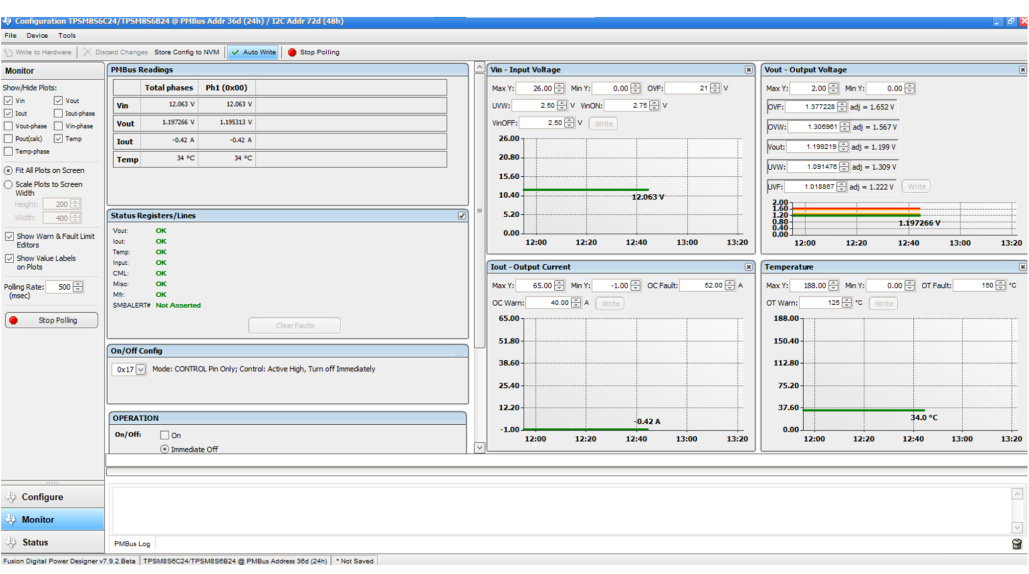
In the interest of monitoring or easier debugging, sometimes buck regulators with digital interfaces like PMBus are preferred in ATE power design, especially for higher-current rails. By using buck regulators with a PMBus interface with telemetry, the real-time output voltage can easily be monitored and the voltage can be adjusted with high accuracy. The graphical user interface (GUI) allows various parameters like temperature and output current to be monitored and different responses can be set for over warn and over fault. This tool is found in the Fusion Digital Power Designer tool page. Figure 7 shows the GUI screen where the specifications can be changed and the DC/DC regulator can be modified.
Thus, PMBus can be an attractive option even if the FPGA in question does not use PMBus to communicate with the DC/DC module. Instead of having to adjust passives, the designer can change parameters digitally during the prototyping and testing phase, and ultimately set all the external passives to control operation with pin-strapping when the board is finally spun. This can save quite a bit of soldering time and headache during the prototyping process, saving time and money in development.
TPSM8S6C24 is TI’s latest 35A buck module with PMBus and telemetry plus extended security, also an input voltage range from 2.95V to 16V, output voltage 0.5V to 3.6V. The extended security feature minimizes the threats of mistaken or malicious write-commands by providing write lock protection, without the need of any hardware redesign and with minimal firmware modifications. See Extended Security Features in TPS546D24S and TPSM8S6C24 for details of extended security features.
 Figure 7 Monitor Screen
Conclusion
Designing power supplies for ATE requires consideration of design size, noise emissions, efficiency, and power parameter monitoring. TI's broad portfolio of buck modules and converters is well-equipped to address all of these power design challenges from 3A to 140A load current requirements.