Power Stage Gain and Slope Compensation Measurement in PCM (Peak Current Mode) BUCK Converter
Power Stage Gain and Slope Compensation Measurement in PCM (Peak Current Mode) BUCK Converter
Trademarks
All other trademarks are the property of their respective owners.
1 Introduction
PCM (Peak Current Mode) architecture is widely used in DC/DC converters. PCM architecture provides good performance and ease of compensation. Power stage gain and slope compensation play important roles in the PCM BUCK converter. They can suppress subharmonic oscillation and keep the control loop stable. With these parameters, you can deeply optimize power supply and ensure performance in mass production. Usually, the typical power stage gain value is provided in the datasheet, but the slope compensation is seldom provided since it is integrated.
2 Unified PCM BUCK Converter
Figure 1 shows a PCM Buck converter, which is usually composed of several key blocks. It includes the following:
- Error Amplifier (EA)
- PWM Comparator (PWM)
- Slope Compensation (SLP)
- Current Sensing (CS)
- Clock (CLK)
- Power Stage
- Output Stage
The RC network after error amplifier compensates for the output pole and increases loop gain for stability. Typically, Figure 1 can explain PCM BUCK converters.
 Figure 1. PCM BUCK Converter Block Diagram
 During normal operation, the voltage difference between the internal reference voltage (Vref) and the feedback voltage (VFB) is amplified and outputs at COMP node. The clock signal (CLK) turns on high-side FET. The sensed current (CS) compares with the COMP voltage minus slope compensation (SLP) and the output logic is set to turn off high-side FET. The low-side FET turns on for the rest of the period.
Assuming the operating frequency is fixed, the slope compensation is linear, and the COMP is a pin that you can use to measure its voltage at this node. The whole application is explained based on this unified PCM model in CCM (Continuous Current Mode).
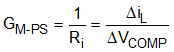
3 Power Stage Gain Measurement
Power Stage Gain (GM-PS) is defined as the gain from COMP voltage (VCOMP) to inductor current (iL). Equation 1 calculates the Power Stage Gain, where Ri is the current sensing gain.