SNLA299 August 2018 LMH0324 , LMH0397 , LMH1208 , LMH1218 , LMH1219 , LMH1297
-
LMH12xx MADI Compatibility Application Note
- Trademarks
- 1 MADI Specification Requirements
- 2
LMH12xx Device Family
- 2.1 LMH12xx Device Family
- 2.2 LMH1218 Device Family Hardware Changes to Support MADI Compatibility
- 2.3 LMH1219 Device Family Recommended Register Settings
- 3 Summary
- 4 References
2.2 LMH1218 Device Family Hardware Changes to Support MADI Compatibility
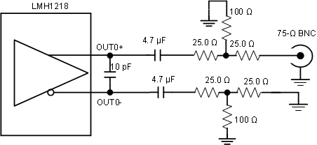
The LMH1218 and LMH0318 devices were first-generation, 12G-SDI cable drivers designed to meet SDI SMPTE requirements. Thus amplitude was designed to be within 800 mV ±10%. Therefore to meet the MADI 300-mV to 600-mV output amplitude, a 6-dB passive attenuator block can be used. If the user wanted to slow down the slew rate in a similar way to the LMH1297 device changes shown in Section 2.1.3, a 10-pF capacitor can be added across OUT0± (see Figure 8).
 Figure 8. LMH1218 Block Diagram
 The following register settings forces raw or CDR bypass for the LMH1218 device:
| RAW | FF | 04 | 07 | //enable retimer registers |
| RAW | 09 | 00 | 20 | //enable override |
| RAW | 1C | 0C | 0C | //out0 and out1 raw data |