SLVAF64A July 2021 – November 2022 TPS62800 , TPS62801 , TPS62802 , TPS62806 , TPS62807 , TPS62808 , TPS62864 , TPS62865 , TPS62866 , TPS62867 , TPS62868 , TPS62869 , TPSM82810 , TPSM82813 , TPSM82816 , TPSM82864A , TPSM82866A , TPSM82866C , TPSM8287A06 , TPSM8287A10 , TPSM8287A15 , TPSM8287B15 , TPSM8287B30
4 TPS62800/1/2/6/7/8: VSEL/MODE Pin
VSEL/MODE pin has a similar structure to VSET/VID pin, but it is used for a different setting. During t_startup_delay, RVSEL resistance set the output voltage value, whereas during operation the pin allows to enable either forced-PWM mode (connect it to a high level) or Power-Save Mode (connect it to a low level) (TPS6280x 1.8-V to 5.5-V, 0.6A / 1-A, 2.3-µA IQ Step Down Converter 6-Pin, 0.35-mm Pitch WCSP Package data sheet).
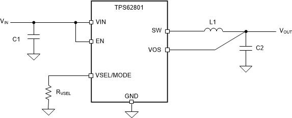
The same considerations made for VSET/VID pin are still valid. If the designer wants to run the device in PSM, the standard configuration can be adopted as shown in Figure 4-1: it is sufficient to place a resistor connected to ground. During t_startup_delay, the R2D conversion can be performed without additional parasitics and during operation it pulls down the pin to GND.
 Figure 4-1 TPS62801 Typical Application Schematics
Instead, if the designer wants to set VSEL/MODE pin to High level (forced-PWM operation), they need to put in parallel to the resistor a driving circuit to properly drive the input.
The preferred solution is to also use an external digital circuit (for example, an FPGA or an MCU) to correctly drive the pin during operation as shown in Figure 4-2. As before, the designer needs to assure that the GPIO parasitics are lower than the maximum ones, as specified in section Section 2.
 Figure 4-2 Typical Application
Schematics, VSEL/MODE Driving Circuit with MCU