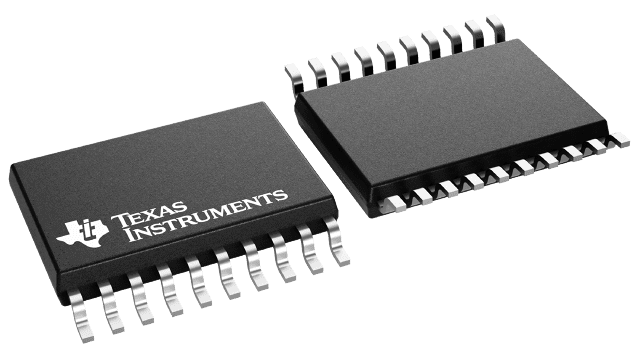
Gehäuseinformationen
| Gehäuse | Pins TSSOP (PW) | 20 |
| Betriebstemperaturbereich (°C) -40 to 85 |
| Gehäusemenge | Träger 70 | TUBE |
Merkmale von BQ77905
- NORMAL mode: 6 µA (BQ77904 and BQ77905)
- Full suite of voltage, current, and temperature protections
- Scalable cell count from 3 series to 20 series or more
- Voltage protection (accuracy ±10 mV)
- Overvoltage: 3 V to 4.575 V
- Undervoltage: 1.2 V to 3 V
- Open cell and open-wire detection (OW)
- Current Protection
- Overcurrent discharge 1: –10 mV to –85 mV
- Overcurrent discharge 2: –20 mV to +170 mV
- Short circuit discharge: –40 mV to +340 mV
- Accuracy ±20% for ≤ 20 mV, ±30% for > 20 mV across full temperature
- Temperature protection
- Overtemperature charge: 45°C or 50°C
- Overtemperature discharge: 65°C or 70°C
- Undertemperature charge: –5°C or 0°C
- Undertemperature discharge: –20°C or –10°C
- Additional Features
- Independent charge (CHG) and discharge (DSG) FET drivers
- 36-V absolute maximum rating per cell input
- Built-in-self-test functions for high reliability
- SHUTDOWN mode: 0.5-µA maximum
- Functional Safety-Capable
Beschreibung von BQ77905
The BQ77904 and BQ77905 devices are low-power battery pack protectors that implement a suite of voltage, current, and temperature protections without microcontroller (MCU) control. The device’s stackable interface provides simple scaling to support battery cell applications from 3 series to 20 series or more. Protection thresholds and delays are factory-programmed and available in a variety of configurations. Separate overtemperature and undertemperature thresholds for discharge (OTD and UTD) and charge (OTC and UTC) are provided for added flexibility.
The device achieves pack protection through the integrated independent CHG and DSG low-side NMOS FET drivers, which may be disabled through two control pins. These control pins may also be used to achieve cell protection solutions for higher series (6 series and beyond) in a simple and economical manner. To do this, simply cascade a higher device CHG and DSG outputs to the immediate lower device control pins. For a reduced component count, all protection faults use internal delay timers.
