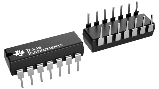
Gehäuseinformationen
| Gehäuse | Pins PDIP (N) | 14 |
| Betriebstemperaturbereich (°C) -55 to 125 |
| Gehäusemenge | Träger 25 | TUBE |
Merkmale von CD4066B
- 15V digital or ±7.5V peak-to-peak switching
- 125Ω typical on-state resistance for 15V operation
- Switch on-state resistance matched to within 5Ω over 15V signal-input range
- On-state resistance flat over full peak-to-peak signal range
- High on or off output-voltage ratio: 80dB typical at fis = 10kHz, RL = 1kΩ
- High degree of linearity: <0.5% distortion typical at fis = 1kHz, Vis = 5Vp-p VDD – VSS ≥ 10V, RL = 10kΩ
- Extremely low off-state switch leakage, resulting in very low offset current and high effective off-state resistance: 10 pA typical at VDD – VSS = 10V, TA = 25°C
- Extremely high control input impedance (control circuit isolated from signal circuit): 1012Ω typical
- Low crosstalk between switches: –50dB typical at fis = 8MHz, RL = 1kΩ
- Matched control-input to signal-output capacitance: reduces output signal transients
- Frequency response, switch On = 40MHz typical
- 100% tested for quiescent current at 20V
- 5V, 10V, and 15V parametric ratings
Beschreibung von CD4066B
The CD4066B device is a quad bilateral switch intended for the transmission or multiplexing of analog or digital signals. It is pin-for-pin compatible with the CD4016B device, but exhibits a much lower on-state resistance. In addition, the on-state resistance is relatively constant over the full signal-input range.
The CD4066B device consists of four bilateral switches, each with independent controls. Wide operating supply of 3V to 18V allows for use in a broad array of applications. The advantages over single-channel switches include peak input-signal voltage swings equal to the full supply voltage and more constant on-state impedance over the input-signal range. However, for sample-and-hold applications, the CD4016B device is recommended.
