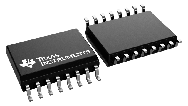
Gehäuseinformationen
| Gehäuse | Pins SOIC (DW) | 16 |
| Betriebstemperaturbereich (°C) -40 to 125 |
| Gehäusemenge | Träger 2.000 | LARGE T&R |
Merkmale von ISO7721-Q1
- Qualified for automotive applications
- AEC-Q100 qualified With the following results:
- Device temperature grade 1: –40°C to +125°C ambient operating temperature range
- Device HBM ESD classification level 3A
- Device CDM ESD classification level C6
-
Functional Safety-Capable
- Documentation available to aid functional safety system design: ISO7720-Q1, ISO7721-Q1
- 100 Mbps data rate
- Robust isolation barrier:
- >30-Year projected lifetime at 1.5 kV RMS working voltage
- Up to 5000 V RMS Isolation Rating
- Up to 12.8 kV surge capability
- ±100 kV/µs Typical CMTI
- Wide supply range: 2.25 V to 5.5 V
- 2.25-V to 5.5-V level translation
- Default output High (ISO772x) and Low (ISO772xF) Options
- Low power consumption, typical 1.7 mA per channel at 1 Mbps
- Low propagation delay: 11 ns typical
- Robust electromagnetic compatibility (EMC)
- System-Level ESD, EFT, and surge immunity
- ±8 kV IEC 61000-4-2 contact discharge protection across isolation barrier
- Low emissions
- Wide-SOIC (DW-16 , DWV-8) and Narrow-SOIC (D-8) package options
- Safety-related Certifications
- VDE reinforced insulation per DIN EN IEC 60747-17 (VDE 0884-17)
- UL 1577 component recognition program
- IEC 62368-1, IEC 61010-1, IEC 60601-1 and GB 4943.1 certifications
Beschreibung von ISO7721-Q1
The ISO772x-Q1 devices are high-performance, dual-channel digital isolators with 5000 V RMS (DW and DWV packages) and 3000 V RMS (D package) isolation ratings per UL 1577. This family includes devices with reinforced insulation ratings according to VDE, CSA, TUV and CQC.
The ISO772x-Q1 devices provide high electromagnetic immunity and low emissions at low power consumption, while isolating CMOS or LVCMOS digital I/Os. Each isolation channel has a logic input and output buffer separated by a double capacitive silicon dioxide (SiO 2) insulation barrier. The ISO7720-Q1 device has both channels in the same direction while the ISO7721-Q1 device has both channels in the opposite direction. In the event of input power or signal loss, the default output is high for devices without suffix F and low for devices with suffix F. See the Device Functional Modes section for further details.
Used in conjunction with isolated power supplies, these devices help prevent noise currents on data buses, such as CAN and LIN, from damaging sensitive circuitry. Through innovative chip design and layout techniques, the electromagnetic compatibility of the ISO772x-Q1 devices has been significantly enhanced to ease system-level ESD, EFT, surge, and emissions compliance. The ISO772x-Q1 family of devices is available in 16-pin SOIC wide-body (DW) , 8-pin SOIC wide-body (DWV), and 8-pin SOIC narrow-body (D) packages.
