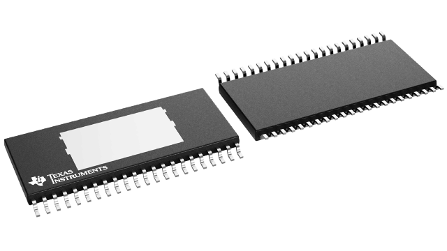
Gehäuseinformationen
| Gehäuse | Pins HTSSOP (DDV) | 44 |
| Betriebstemperaturbereich (°C) 0 to 125 |
| Gehäusemenge | Träger 35 | TUBE |
Merkmale von TAS5612LA
- PurePath™ HD Integrated Feedback Provides:
- 0.05% THD at 1 W Into 4 Ω
- > 65-dB PSRR (No Input Signal)
- > 105-dB (A Weighted) SNR
- Preclipping Output for Control of a Class-G Power
Supply - Reduced Heat Sink Size Due to Use of 60-mΩ
Output MOSFET With > 90% Efficiency at Full
Output Power - Output Power at 10% THD+N
- 125-W and 4-Ω BTL Stereo Configuration
- 250-W and 2-Ω in PBTL Mono Configuration
- Output Power at 1% THD+N
- 105-W and 4-Ω BTL Stereo Configuration
- 55-W and 8-Ω BTL Stereo Configuration
- Click- and Pop-Free Start-up
- Error Reporting Self-Protected Design With UVP,
Overtemperature, and Short-Circuit Protection - EMI Compliant When Used With Recommended
System Design - 44-Pin HTSSOP (DDV) Package for Reduced
Board Size
Beschreibung von TAS5612LA
The TAS5612LA is a feature optimized class-D power amplifier based on the TAS5612A.
The TAS5612LA uses large MOSFETs for improved power efficiency and a novel gate drive scheme for reduced losses in idle and at low output signals leading to reduced heat sink size.
The unique preclipping output signal can be used to control a class-G power supply. This combined with the low idle loss and high power efficiency of the TAS5612LA leads to industry-leading levels of efficiency ensuring a super "green" system.
The TAS5612LA uses constant voltage gain. The internally matched gain resistors ensure a high Power Supply Rejection Ratio giving an output voltage only dependent on the audio input voltage and free from any power supply artifacts.
The high integration of the TAS5612LA makes the amplifier easy to use; and, using TI’s reference schematics and PCB layouts leads to fast design in time. The TAS5612LA is available in the space-saving, surface-mount, 44-pin HTSSOP package.
