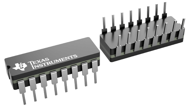
パッケージ情報
| パッケージ | ピン数 CDIP (J) | 16 |
| 動作温度範囲 (℃) -55 to 125 |
| パッケージ数量 | キャリア 25 | TUBE |
CD4044B-MIL の特徴
- 3-state outputs with common output ENABLE
- Separate SET and RESET inputs for each latch
- NOR and NAND configurations
- 5-V, 10-V, and 15-V parametric ratings
- Standardized symmetrical output characteristics
- 100% tested for quiescent current at 20 V
- Maximum input current of 1 µA at 18 V over full package temperature range; 100 nA at 18 V and 25°C
- Noise margin (over full package temperature range):
- 1 V at VDD = 5 V
- 2 V at VDD = 10 V
- 2.5 V at VDD = 15 V
- Meets all requirements of JEDEC Tentative Standard No. 13B, "Standard Specifications for Description of 'B' Series CMOS Devices"
- Applications
- Holding register in multi-register system
- Four bits of independent storage with output ENABLE
- Strobed register
- General digital logic
- CD4043B for positive logic systems
- CD4044B for negative logic systems
Data sheet acquired from Harris Semiconductor
CD4044B-MIL に関する概要
CD4043B types are quad cross-coupled 3-state CMOS NOR latches and the CD4044B types are quad cross-coupled 3-state CMOS NAND latches. Each latch has a separate Q output and individual SET and RESET inputs. The Q outputs are controlled by a common ENABLE input. A logic "1" or high on the ENABLE input connects the latch states to the Q outputs. A logic "0" or low on the ENABLE input disconnects the latch states from the Q outputs, resulting in an open circuit condition on the Q outputs. The open circuit feature allows common busing of the outputs.
The CD4043B and CD4044B types are supplied in 16-lead hermetic dual-in-line ceramic packages (F3A suffix), 16-lead dual-in-line plastic packages (E suffix), 16-lead small-outline package (D, DR, DT, DWR, and NSR suffixes), and 16-lead thin shrink small-outline packages (PW and PWR suffixes).
