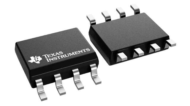
パッケージ情報
| パッケージ | ピン数 SOIC (D) | 8 |
| 動作温度範囲 (℃) -40 to 85 |
| パッケージ数量 | キャリア 75 | TUBE |
TLC3545 の特徴
- 200-KSPS Sampling Rate
- Built-In Conversion Clock
- INL: ±1 LSB Max
DNL: ±1 LSB Max - SINAD = 81.5 dB, SFDR = 95 dB
THD = 94 dB at 15 kHz fin, 200 KSPS - SPI/DSP-Compatible Serial Interfaces With SCLK Input up to 15 MHz
- Single 5-V Supply
- Rail-to-Rail Analog Input With 500 kHz BW
- Two Input Options Available:
- TLC3541 – Single Channel Input
- TLC3545 – Single Channel, Pseudo-Differential Input
- (TLC3541) Optimized DSP Interface – Requires FS Input Only
- Low Power With Auto-Power Down
- Operating Current: 3.5 mA
- Auto-Powerdown Current: 5 uA
- Pin Compatible 12-/14-/16-Bit Family in 8-Pin SOIC and MSOP Packages
- APPLICATIONS
- ATE System
- Industrial Process Control
- Measurement
- Motor Control
TLC3545 に関する概要
The TLC3541 and TLC3545 are a family of high performance, 14-bit, low power, miniature CMOS analog-to-digital converters (ADCs). These devices operate from a single 5-V supply. Devices are available with single, dual, or single pseudo-differential inputs. All of these devices have a chip select (CS)\, serial clock (SCLK), and serial data output (SDO) that provides a direct 3-wire interface to the serial port of most popular host microprocessors (SPI interface). When interfaced with a DSP, a frame sync signal (FS) is used to indicate the start of a serial data frame on either pin 1 (CS)\ or pin 7 (FS) for the TLC3541. The TLC3545 ADC connects to the DSP via pin 1 only (CS)\.
The TLC3541 and TLC3545 are designed to operate with low power consumption. The power saving feature is further enhanced with an auto-power down mode. This product family features a high-speed serial link to modern host processors with an external SCLK up to 15 MHz. Both families use a built-in oscillator as the conversion clock, providing a 2.67 us maximum conversion time.
