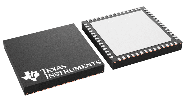
封裝資訊
| 封裝 | 針腳 VQFN (RTQ) | 56 |
| 操作溫度範圍 (°C) -40 to 85 |
| 包裝數量 | 運送業者 250 | SMALL T&R |
ADC3442 的特色
- Quad Channel
- 14-Bit Resolution
- Single Supply: 1.8 V
- Serial LVDS Interface
- Flexible Input Clock Buffer With Divide-by-1, -2, -4
- SNR = 72.4 dBFS, SFDR = 87 dBc at
fIN = 70 MHz - Ultra-Low Power
Consumption:
- 98 mW/Ch at 125 MSPS
- Channel Isolation: 105 dB
- Internal Dither and Chopper
- Support for Multi-Chip Synchronization
- Pin-to-Pin Compatible With 12-Bit Version
- Package: VQFN-56 (8 mm × 8 mm)
ADC3442 的說明
The ADC344x devices are a high-linearity, ultra-low power, quad-channel, 14-bit, 25-MSPS to 125-MSPS, analog-to-digital converter (ADC) family. The devices are designed specifically to support demanding, high input frequency signals with large dynamic range requirements. An input clock divider allows more flexibility for system clock architecture design while the SYSREF input enables complete system synchronization.
The ADC344x family supports serial low-voltage differential signaling (LVDS) to reduce the number of interface lines, thus allowing for high system integration density. The serial LVDS interface is two-wire, where each ADC data are serialized and output over two LVDS pairs. Optionally, a one-wire serial LVDS interface is available. An internal phase-locked loop (PLL) multiplies the incoming ADC sampling clock to derive the bit clock that is used to serialize the 14-bit output data from each channel. In addition to the serial data streams, the frame and bit clocks are transmitted as LVDS outputs.
