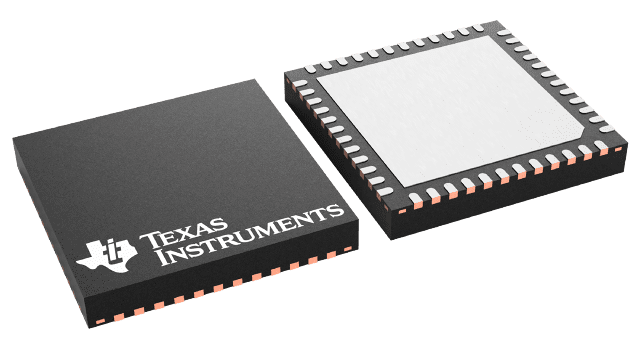
封裝資訊
| 封裝 | 針腳 VQFN (RGZ) | 48 |
| 操作溫度範圍 (°C) -40 to 85 |
| 包裝數量 | 運送業者 2,500 | LARGE T&R |
ADS6148 的特色
- Maximum Sample Rate: 250 MSPS
- 14-Bit Resolution — ADS614X
- 12-Bit Resolution — ADS612X
- 687 mW Total Power Dissipation at 250 MSPS
- Double Data Rate (DDR) LVDS and Parallel CMOS Output Options
- Programmable Fine Gain up to 6dB for SNR/SFDR Trade-Off
- DC Offset Correction
- Supports Input Clock Amplitude Down to 400 mVPP Differential
- Internal and External Reference Support
- 48-QFN Package (7mm × 7mm)
- Pin Compatible with ADS5547 Family
- APPLICATIONS
- Multicarrier, Wide Band-Width Communications
- Wireless Multi-carrier Communications Infrastructure
- Software Defined Radio
- Power Amplifier Linearization
- 802.16d/e
- Test and Measurement Instrumentation
- High Definition Video
- Medical Imaging
- Radar Systems
ADS6148 的說明
ADS614X (ADS612X) is a family of 14-bit (12-bit) A/D converters with sampling rates up to 250 MSPS. It combines high dynamic performance and low power consumption in a compact 48 QFN package. This makes it well-suited for multicarrier, wide band-width communications applications.
ADS614X/2X has fine gain options that can be used to improve SFDR performance at lower full-scale input ranges. It includes a dc offset correction loop that can be used to cancel the ADC offset. Both DDR LVDS (Double Data Rate) and parallel CMOS digital output interfaces are available. At lower sampling rates, the ADC automatically operates at scaled down power with no loss in performance.
It includes internal references while the traditional reference pins and associated decoupling capacitors have been eliminated. Nevertheless, the device can also be driven with an external reference. The device is specified over the industrial temperature range (-40°C to 85°C).
