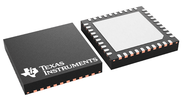
封裝資訊
| 封裝 | 針腳 VQFN (RHA) | 40 |
| 操作溫度範圍 (°C) -40 to 85 |
| 包裝數量 | 運送業者 250 | SMALL T&R |
CC2540 的特色
- True Single-Chip BLE Solution: CC2540 Can Run Both Application and BLE Protocol
Stack, Includes Peripherals to Interface With Wide Range of Sensors, Etc. - 6-mm × 6-mm Package
- RF
- Bluetooth low energy technology Compatible
- Excellent Link Budget (up to 97 dB), Enabling Long-Range
Applications Without External Front End - Accurate Digital Received Signal-Strength Indicator (RSSI)
- Suitable for Systems Targeting Compliance With Worldwide
Radio Frequency Regulations: ETSI EN 300 328 and
EN 300 440 Class 2 (Europe), FCC CFR47
Part 15 (US), and ARIB STD-T66 (Japan)
- Layout
- Few External Components
- Reference Design Provided
- 6-mm × 6-mm QFN40 Package
- Low Power
- Active Mode RX Down to 19.6 mA
- Active Mode TX (–6 dBm): 24 mA
- Power Mode 1 (3-µs Wake-Up): 235 µA
- Power Mode 2 (Sleep Timer On): 0.9 µA
- Power Mode 3 (External Interrupts): 0.4 µA
- Wide Supply Voltage Range (2 V–3.6 V)
- Full RAM and Register Retention in All Power Modes
- TPS62730 Compatible
Low Power in Active Mode- RX Down to 15.8 mA (3 V Supply)
- TX (-6 dBm): 18.6 mA (3 V Supply)
- Microcontroller
- High-Performance and Low-Power 8051 Microcontroller Core
- In-System-Programmable Flash, 128 KB or 256 KB
- 8-KB SRAM
- Peripherals
- 12-Bit ADC with Eight Channels and Configurable Resolution
- Integrated High-Performance Op-Amp and Ultralow-Power Comparator
- General-Purpose Timers (One 16-Bit, Two 8-Bit)
- 21 General-Purpose I/O Pins (19× 4 mA, 2× 20 mA)
- 32-kHz Sleep Timer With Capture
- Two Powerful USARTs With Support for Several Serial Protocols
- Full-Speed USB Interface
- IR Generation Circuitry
- Powerful Five-Channel DMA
- AES Security Coprocessor
- Battery Monitor and Temperature Sensor
- Each CC2540 Contains a Unique 48-bit IEEE Address
- Software Features
- Bluetooth v4.0 Compliant Protocol Stack
for Single-Mode BLE Solution- Complete Power-Optimized Stack, Including Controller and
Host- GAP – Central, Peripheral, Observer, or Broadcaster
(Including Combination Roles) - ATT / GATT – Client and Server
- SMP – AES-128 Encryption and Decryption
- L2CAP
- GAP – Central, Peripheral, Observer, or Broadcaster
- Sample Applications and Profiles
- Generic Applications for GAP Central and Peripheral Roles
- Proximity, Accelerometer, Simple Keys, and Battery GATT Services
- Multiple Configuration options
- Single-Chip Configuration, Allowing Application to Run on CC2540
- Network Processor Interface for Applications Running on an External Microcontroller
- BTool – Windows PC Application for Evaluation, Development, and Test
- Complete Power-Optimized Stack, Including Controller and
- Development Tools
- CC2540 Mini Development Kit
- SmartRF Software
- Supported by IAR Embedded Workbench Software for 8051
- Bluetooth v4.0 Compliant Protocol Stack
- 2.4-GHz Bluetooth low energy Systems
- Mobile Phone Accessories
- Sports and Leisure Equipment
- Consumer Electronics
- Human Interface Devices (Keyboard, Mouse, Remote Control)
- USB Dongles
- Health Care and Medical
- TPS62730 is a 2 MHz Step Down Converter with Bypass Mode
- Extends Battery Lifetime by up to 20%
- Reduced Current in TX and RX
- 30 nA Bypass Mode Current to Support Low Power Modes
- RF Performance Unchanged
- Small Package Allows for Small Solution Size
- CC2540 Controllable
All other trademarks are the property of their respective owners
CC2540 的說明
The CC2540 is a cost-effective, low-power, true system-on-chip (SoC) for Bluetooth low energy applications. It enables robust BLE master or slave nodes to be built with very low total bill-of-material costs. The CC2540 combines an excellent RF transceiver with an industry-standard enhanced 8051 MCU, in-system programmable flash memory, 8-KB RAM, and many other powerful supporting features and peripherals. The CC2540 is suitable for systems where very low power consumption is required. Very low-power sleep modes are available. Short transition times between operating modes further enable low power consumption.
The CC2540 comes in two different versions: CC2540F128/F256, with 128 and 256 KB of flash memory, respectively.
Combined with the Bluetooth low energy protocol stack from Texas Instruments, the CC2540F128/F256 forms the market’s most flexible and cost-effective single-mode Bluetooth low energy solution.
