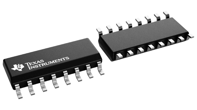
封裝資訊
| 封裝 | 針腳 SOIC (D) | 16 |
| 操作溫度範圍 (°C) -55 to 125 |
| 包裝數量 | 運送業者 2,500 | LARGE T&R |
CD4053B 的特色
- Wide range of digital and analog
signal levels:
- Digital: 3 V to 20 V
- Analog: ≤ 20 V P-P
- Low ON resistance, 125 Ω (typical) over 15 V P-P signal input range for V DD – V EE = 18 V
- High OFF resistance, channel leakage of ±100 pA (typical) at V DD – V EE = 18 V
- Logic-level conversion for digital addressing signals of 3 V to 20 V (V DD – V SS = 3 V to 20 V) to switch analog signals to 20 V P-P (V DD – V EE = 20 V) matched switch characteristics, r ON = 5 Ω (typical) for V DD – V EE = 15 V very low quiescent power dissipation under all digital-control input and supply conditions, 0.2 µW (typical) at V DD – V SS = V DD – V EE = 10 V
- Binary address decoding on chip
- 5 V, 10 V, and 15 V parametric ratings
- 100% tested for quiescent current at 20 V
- Maximum input current of 1 µA at 18 V over full package temperature range, 100 nA at 18 V and 25°C
- Break-before-make switching eliminates channel overlap
CD4053B 的說明
The CD405xB analog multiplexers and demultiplexers are digitally-controlled analog switches having low ON impedance and very low OFF leakage current. These multiplexer circuits dissipate extremely low quiescent power over the full V DD – V SS and V DD – V EE supply-voltage ranges, independent of the logic state of the control signals.
