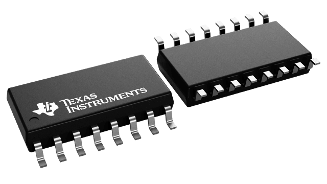
封裝資訊
| 封裝 | 針腳 SOP (NS) | 16 |
| 操作溫度範圍 (°C) -55 to 125 |
| 包裝數量 | 運送業者 2,000 | LARGE T&R |
CD4511B 的特色
- High-output-sourcing capability............up to 25 mA
- Input latches for BCD Code storage
- Lamp Test and Blanking capability
- 7-segment outputs blanked for BCD input codes > 1001
- 100% tested for quiescent current at 20 V
- Max. input current of 1 µA at 18 V, over full package-temperature range, 100 nA at 18 V and 25°C
- 5-V, 10-V, and 15-V parametric ratings
- Applications
- Driving common-cathode LED displays
- Multiplexing with common-cathode LED displays
- Driving incandescent displays
- Driving low-voltage fluorescent displays
CD4511B 的說明
CD4511B types are BCD-to-7-segment latch decoder drivers constructed with CMOS logic and n-p-n bipolar transistor output devices on a single monolithic structure. These devices combine the low quiescent power dissipation and high noise immunity features of RCA CMOS with n-p-n bipolar output transistors capable of sourcing up to 25 MA. This capability allows the CD4511B types to drive LED's and other displays directly.
Lamp Test (LT)\, Blanking (BL)\, and Latch Enable or Strobe inputs are provided to test the display, shut off or intensity-modulate it, and store or strobe a BCD code, respectively. Several different signals may be multiplexed and displayed when external multiplexing circuitry is used.
The CD4511B types are supplied in 16-lead hermetic dual-in-line ceramic packages (F3A suffix), 16-lead dual-in-line plastic packages (E suffix), 16-lead small-outline packages (NSR suffix), and 16-lead thin shrink small-outline packages (PW and PWR suffixes).
These devices are similar to the type MC14511.
