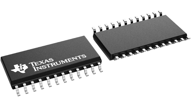
封裝資訊
| 封裝 | 針腳 SOIC (DW) | 24 |
| 操作溫度範圍 (°C) -55 to 125 |
| 包裝數量 | 運送業者 2,000 | LARGE T&R |
CD4515B 的特色
CD4515B Output "Low" on Select
- Strobed input latch
- Inhibit control
- 100% tested for quiescent current at 20 V
- Maximum input current of 1 µA at 18 V over full package-temperature range; 100 nA at 18 V and 25°C
- Noise margin (over full package temperature range):
- 1 V at VDD = 5 V
- 2 V at VDD = 10 V
- 2.5 V at VDD = 15 V
- 5-V, 10-V, and 15-V parametric ratings
- Standardized, symmetrical output characteristics
- Meets all requirements of JEDEC Tentative Standard No. 13B, "Standard Specifications for Description of ’B’ Series CMOS Devices"
- Applications:
- Digital multiplexing
- Address decoding
- Hexadecimal/BCD decoding
- Program-counter decoding
- Control decoder
Data sheet acquired from Harris Semiconductor.
CD4515B 的說明
CD4514B and CD4515B consist of a 4-bit strobed latch and a 4-to-16-line decoder. The latches hold the last input data presented prior to the strobe transition from 1 to 0. Inhibit control allows all outputs to be placed at 0 (CD4514B) or 1 (CD4515B) regardless of the state of the data or strobe inputs.
The decode truth table indicates all combinations of data inputs and appropriate selected outputs.
These devices are similar to industry types MC14514 and MC14515.
The CD4514B and CD4515B types are supplied in 16-lead hermetic dual-in-line ceramic packages (F3A suffix), 16-lead dual-in-line plastic packages (E suffix), and 16-lead small-outline packages (M and M96 suffixes).
