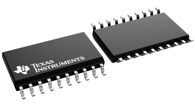
封裝資訊
| 封裝 | 針腳 SOIC (DW) | 20 |
| 操作溫度範圍 (°C) -40 to 85 |
| 包裝數量 | 運送業者 25 | TUBE |
SN74AC563 的特色
- 2-V to 6-V VCC Operation
- Inputs Accept Voltages to 6 V
- Max tpd of 9 ns at 5 V
- 3-State Inverting Outputs Drive Bus Lines Directly
- Full Parallel Access for Loading
- Flow-Through Architecture to Optimize PCB Layout
SN74AC563 的說明
The ’AC563 devices are octal D-type transparent latches with 3-state outputs. When the latch-enable (LE) input is high, the Q\ outputs follow the complements of the data (D) inputs. When LE is taken low, the Q\ outputs are latched at the inverse logic levels set up at the D inputs.
A buffered output-enable (OE)\ input can be used to place the eight outputs in either a normal logic state (high or low logic levels) or the high-impedance state. In the high-impedance state, the outputs neither load nor drive the bus lines significantly. The high-impedance state and increased drive provide the capability to drive bus lines without need for interface or pullup components.
(OE)\ does not affect internal operations of the latches. Old data can be retained or new data can be entered while the outputs are in the high-impedance state.
To ensure the high-impedance state during power up or power down, OE\ should be tied to VCC through a pullup resistor; the minimum value of the resistor is determined by the current-sinking capability of the driver.
