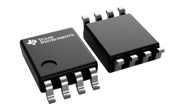
封裝資訊
| 封裝 | 針腳 VSSOP (DCU) | 8 |
| 操作溫度範圍 (°C) -40 to 85 |
| 包裝數量 | 運送業者 3,000 | LARGE T&R |
SN74CB3Q3306A 的特色
- High-Bandwidth Data Path (up to 500 MHz(1))
- 5-V-Tolerant I/Os With Device Powered Up or Powered Down
- Low and Flat ON-State Resistance (ron) Characteristics Over
Operating Range (ron = 4 Ω Typ) - Rail-to-Rail Switching on Data I/O Ports
- 0- to 5-V Switching With 3.3-V VCC
- 0- to 3.3-V Switching With 2.5-V VCC
- Bidirectional Data Flow With Near-Zero Propagation Delay
- Low Input/Output Capacitance Minimizes Loading and Signal Distortion
(Cio(OFF) = 3.5 pF Typ) - Fast Switching Frequency (f OE = 20 MHz Max)
- Data and Control Inputs Provide Undershoot Clamp Diodes
- Low Power Consumption (ICC = 0.25 mA Typ)
- VCC Operating Range From 2.3 V to 3.6 V
- Data I/Os Support 0- to 5-V Signaling Levels
(0.8 V, 1.2 V, 1.5 V, 1.8 V, 2.5 V, 3.3 V, 5 V) - Control Inputs Can Be Driven by TTL or 5-V/3.3-V CMOS Outputs
- Ioff Supports Partial-Power-Down Mode Operation
- Latch-Up Performance Exceeds 100 mA Per JESD 78, Class II
- ESD Performance Tested Per JESD 22
- 2000-V Human-Body Model (A114-B, Class II)
- 1000-V Charged-Device Model (C101)
- Supports Both Digital and Analog Applications: USB Interface, Differential Signal
Interface, Bus Isolation, Low-Distortion Signal Gating
(1) For additional information regarding the performance characteristics of the CB3Q family, refer to the TI application report, CBT-C, CB3T, and CB3Q Signal-Switch Families, literature number SCDA008.
SN74CB3Q3306A 的說明
The SN74CB3Q3306A is a high-bandwidth FET bus switch utilizing a charge pump to elevate the gate voltage of the pass transistor, providing a low and flat ON-state resistance (ron). The low and flat ON-state resistance allows for minimal propagation delay and supports rail-to-rail switching on the data input/output (I/O) ports. The device also features low data I/O capacitance to minimize capacitive loading and signal distortion on the data bus. Specifically designed to support high-bandwidth applications, the SN74CB3Q3306A provides an optimized interface solution ideally suited for broadband communications, networking, and data-intensive computing systems.
The SN74CB3Q3306A is organized as two 1-bit switches with separate output-enable (1OE, 2OE) inputs. It can be used as two 1-bit bus switches or as one 2-bit bus switch. When OE is low, the associated 1-bit bus switch is ON and the A port is connected to the B port, allowing bidirectional data flow between ports. When OE is high, the associated 1-bit bus switch is OFF, and a high-impedance state exists between the A and B ports.
This device is fully specified for partial-power-down applications using Ioff. The Ioff circuitry prevents damaging current backflow through the device when it is powered down. The device has isolation during power off.
To ensure the high-impedance state during power up or power down, OE should be tied to VCC through a pullup resistor; the minimum value of the resistor is determined by the current-sinking capability of the driver.
