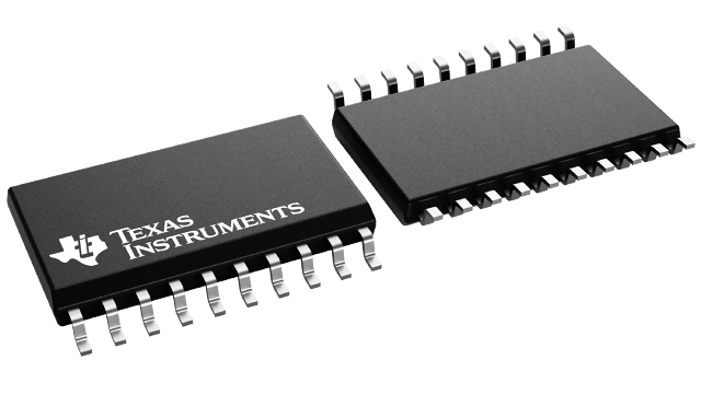
封裝資訊
| 封裝 | 針腳 SOIC (DW) | 20 |
| 操作溫度範圍 (°C) -40 to 85 |
| 包裝數量 | 運送業者 25 | TUBE |
TLV2556 的特色
- 12-Bit Resolution Analog-to-Digital Converter
(ADC) - Up to 200-kSPS (150-kSPS for 3 V) Throughput
Over Operating Temperature Range With 12-Bit
Output Mode - 11 Analog Input Channels
- Three Built-In Self-Test Modes
- Inherent Sample and Hold Function
- Programmable Reference Source (2.048 / 4.096 V
Internal or External) - Inherent Sample and Hold Function
- Linearity Error of ±1 LSB (Maximum)
- On-Chip Conversion Clock
- Programmable Conversion Status Output: INT
or EOC - Unipolar or Bipolar Output Operation
- Programmable Most Significant Bit (MSB) or Least
Significant Bit (LSB) First - Programmable Power Down
- Programmable Output Data Length
- SPI-Compatible Serial Interface With I/O Clock
Frequencies Up to 15 MHz (CPOL = 0,
CPHA = 0)
TLV2556 的說明
The TLV2556 device is a 12-bit switched-capacitor successive-approximation analog-to-digital converter (ADC). The ADC has three control inputs: chip select (CS), the input-output clock, and the address and control input (DATAIN). These inputs communicate with the serial port of a host processor or peripheral through a serial 3-state output.
In addition to the high-speed converter and versatile control capability, the device has an on-chip 14-channel multiplexer that can select any one of 11 inputs or any one of three internal self-test voltages using configuration register 1. The sample-and-hold function is automatic. At the end of conversion, when programmed as EOC, the pin 19 output goes high to indicate that conversion is complete. If pin 19 is programmed as INT, the signal goes low when the conversion is complete. The converter incorporated in the device features differential, high-impedance reference inputs that facilitate ratiometric conversion, scaling, and isolation of analog circuitry from logic and supply noise. A switched-capacitor design allows low error conversion over the full operating temperature range. An internal reference is available and its voltage level is programmable through configuration register 2 (CFGR2).
The TLV2556 is characterized for operation from TA = –40°C to +85°C.
