SLVA469D June 2013 – January 2023 TLV62130 , TLV62130A , TLV62150 , TLV62150A , TPS61175 , TPS61175-Q1 , TPS62130 , TPS62130A , TPS62131 , TPS62132 , TPS62133 , TPS62135 , TPS62136 , TPS62140 , TPS62140A , TPS62141 , TPS62142 , TPS62143 , TPS62150 , TPS62150A , TPS62151 , TPS62152 , TPS62153 , TPS62160 , TPS62161 , TPS62162 , TPS62163 , TPS62170 , TPS62171 , TPS62172 , TPS62173
1.1 Concept
The inverting buck-boost topology is very similar to the buck topology. In a standard buck configuration, shown in Figure 1-1, the positive connection (VOUT) is connected to the inductor and the return connection is connected to the device ground.
 Figure 1-1 Buck Topology
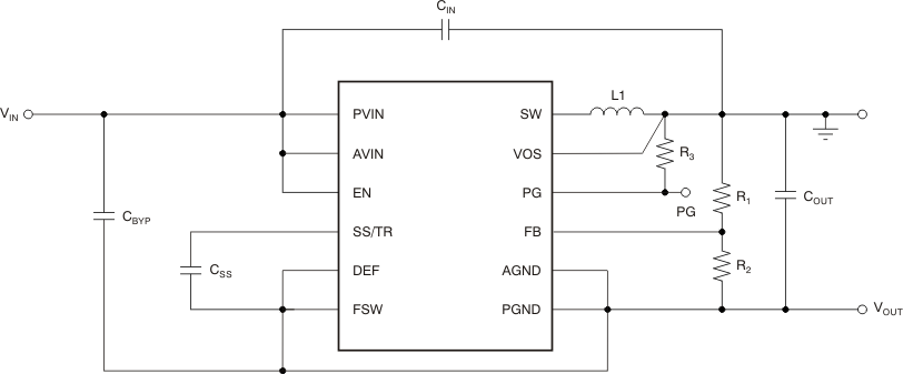
However, in the inverting buck-boost configuration illustrated in Figure 1-2, the device ground is used as the negative output voltage pin (labeled as VOUT). What was previously the positive output in the buck configuration is now used as the ground (GND). This shift in topology allows the output voltage to be inverted and always remain lower than the ground.
 Figure 1-2 Inverting Buck-Boost Topology
The circuit operation in the inverting buck-boost topology differs from that in the buck topology. Though the components are connected the same as with a buck converter, the output voltage terminals are reversed, as Figure 1-3(a) shows. During the on time of the control MOSFET, shown in Figure 1-3(b), the inductor is charged with current, while the output capacitor supplies the load current. The inductor does not provide current to the load during that time. During the off time of the control MOSFET and the on time of the synchronous MOSFET, shown in Figure 1-3(c), the inductor provides current to the load and the output capacitor. These changes affect many parameters, as discussed in the Design Considerations section.
 Figure 1-3 Buck-Boost Configuration