SLVAF89 November 2021 TLV61046A , TLV61048 , TPS61040 , TPS61041 , TPS61045 , TPS61046 , TPS61085 , TPS61086 , TPS61088 , TPS61089 , TPS61096A , TPS61170 , TPS61175 , TPS61178 , TPS61288
2 Requirements of External Bias for Boost Converters
To figure out the requirements of supporting external bias, it is necessary to analyze the control strategy of these boost converters. According to the different main control strategies, middle-voltage boost converters (output voltages above 7 V) can be divided into three control strategies.
The first type is fixed frequency control (PWM), a relatively simple and commonly-used control strategy. The devices using this control strategy include the TPS61175, TPS61178, and so forth.
The second type is quasi-constant frequency control, or constant on or off time (COT) control. The constant off time control device will calculate an off time Toff based on the input voltage and output voltage to keep the frequency basically constant. The devices using this control strategy include the TPS61089, TPS61372, and so forth.
The third type is the pulse-frequency modulation control (PFM). There are fewer devices using PFM, including the TPS61096a and TPS61040.
For COT control, the device needs to sample input voltage to calculate Toff or Ton. There are also two methods to sample input voltage:
- Directly sample the VIN pin voltage
- Sample the average voltage of the SW pin, which is almost the same as Vin.
The derivation process is as follows:
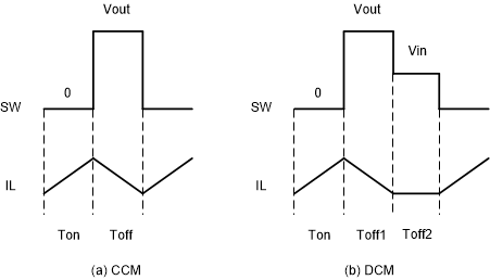
The voltage waveforms of SW in CCM and DCM are shown in Figure 2-1.
 Figure 2-1 Waveforms of Boost SW Voltage in CCM
and DCM
Figure 2-1 Waveforms of Boost SW Voltage in CCM
and DCMFor CCM, the average voltage of the SW pin is calculated with Equation 1:
where
- D is the switching duty cycle
- TS is the switching period
For DCM, the Ton and Toff1 are determined with Equation 2:
where
- L is the inductance of power inductor
- Ipeak is the peak current of inductor
The average voltage of the SW pin is calculated with Equation 3:
Note that the device needs to sample the voltage of the SW pin to calculate a proper Toff and Ton. For external bias applications, the boost converter will not work as desired if the device samples the voltage of the VIN pin, signal Vin. For example, the working frequency of the TPS61087 will increase as the input voltage increases in CCM. This is because the Toff remains unchanged with external bias, while the required duty cycle reduces as the input voltage rises, so Ton decreases. Thus, the first and most important requirement of external bias is that the boost converter must sample power Vin for Toff and Ton calculation if the COT control strategy is used.
The second requirement is that the boost converter has no load disconnection function or the function is not used in a practical application. Consider the TPS61372 as an example. It integrates a P-channel MOSFET connected in series with a high-side MOSFET. If the power Vin is high, the source voltage of the isolated PMOS on the output side is high. The device may not be able to generate a sufficiently high gate voltage and the PMOS will not shut down if the signal Vin is low. In addition, the signal Vin may be sampled to determine the driving signal of isolation MOSFET so it may bring abnormal behavior when output sides are shorted. Thus, those devices integrating isolation MOSFET are not recommended for external bias application.
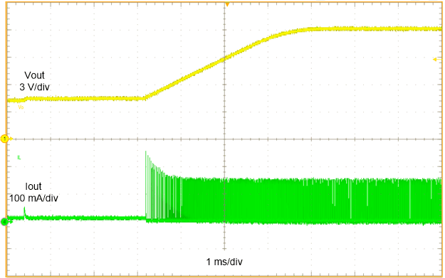
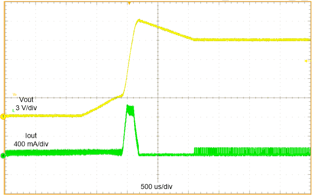
The third requirement is power sequence. Power Vin should be provided before signal Vin to pre-charge the output capacitor. For some devices like the TPS61288 and TPS61089, the start-up will fail and the input sides will be shorted if the power Vin is provided later. This is because the device is already working before start-up and the error amplifier of the device will produce too large an EA output voltage due to 0-V power Vin. This brings almost infinite Ton. Figure 2-2 and Figure 2-3 show different start-up waveforms of the TLV61046a. In Figure 2-2, power Vin is provided first and then signal Vin is provided; while signal Vin is provided first and then power Vin is provided as shown in Figure 2-3. It is obvious that the inrush current of start-up is much larger and the soft-start feature is lost even if the power Vin can be provided later in an external bias application.
 Figure 2-2 TLV61046a Power Vin = Signal Vin = 5
V, Vo = 12 V, Io = 10 mA, Power Vin Provided First
 Figure 2-3 TLV61046a Power Vin = Signal Vin = 5
V, Vo = 12 V, Io = 10 mA, Signal Vin Provided First