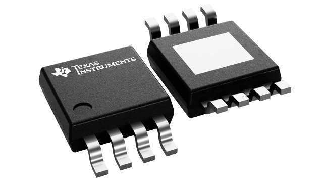
封裝資訊
| 封裝 | 針腳 HVSSOP (DGN) | 8 |
| 操作溫度範圍 (°C) -40 to 85 |
| 包裝數量 | 運送業者 2,500 | LARGE T&R |
TPA6205A1 的特色
- 1.25 W Into 8-Ω From a 5-V Supply at THD = 1%
(Typical) - Shutdown Pin has 1.8-V Compatible Thresholds
- Low Supply Current: 1.7 mA Typical
- Shutdown Current < 10 µA
- Only Five External Components
- Improved PSRR (90 dB) and Wide Supply
Voltage (2.5 V to 5.5 V) for Direct Battery
Operation - Fully Differential Design Reduces RF
Rectification - Improved CMRR Eliminates Two Input
Coupling Capacitors - C(BYPASS) Is Optional Due to Fully Differential
Design and High PSRR
- Improved PSRR (90 dB) and Wide Supply
- Available in 3-mm × 3-mm QFN Package (DRB)
- Available in an 8-Pin PowerPAD™ MSOP (DGN)
- Available in a 2-mm ™ 2-mm MicroStar Junior™
BGA Package (ZQV)
TPA6205A1 的說明
The TPA6205A1 device is a 1.25-W mono fully differential amplifier designed to drive a speaker with at least 8-Ω impedance while consuming less than 37 mm2 (ZQV package option) total printed-circuit-board (PCB) area in most applications. This device operates from 2.5 V to 5.5 V, drawing only 1.7 mA of quiescent supply current. The TPA6205A1 is available in the space-saving 2-mm × 2-mm MicroStar Junior BGA package, and the space saving 3-mm × 3-mm QFN (DRB) package.
Features like 85-dB PSRR from 90 Hz to 5 kHz, improved RF-rectification immunity, and small PCB area makes the TPA6205A1 ideal for wireless handsets. A fast start-up time of 4s with minimal pop makes the TPA6205A1 ideal for PDA applications.
