SLPA021 November 2024 CSD13303W1015 , CSD16301Q2 , CSD16321Q5 , CSD16322Q5 , CSD16323Q3 , CSD16325Q5 , CSD16327Q3 , CSD16340Q3 , CSD16342Q5A , CSD16401Q5 , CSD16403Q5A , CSD16404Q5A , CSD16406Q3 , CSD16407Q5 , CSD16408Q5 , CSD16409Q3 , CSD16410Q5A , CSD16411Q3 , CSD16412Q5A , CSD16413Q5A , CSD16414Q5 , CSD16415Q5 , CSD16556Q5B , CSD17301Q5A , CSD17302Q5A , CSD17303Q5 , CSD17304Q3 , CSD17305Q5A , CSD17306Q5A , CSD17307Q5A , CSD17308Q3 , CSD17309Q3 , CSD17310Q5A , CSD17311Q5 , CSD17312Q5 , CSD17313Q2 , CSD17322Q5A , CSD17327Q5A , CSD17381F4 , CSD17501Q5A , CSD17505Q5A , CSD17506Q5A , CSD17507Q5A , CSD17510Q5A , CSD17522Q5A , CSD17527Q5A , CSD17551Q3A , CSD17551Q5A , CSD17552Q3A , CSD17552Q5A , CSD17553Q5A , CSD17555Q5A , CSD17556Q5B , CSD17559Q5 , CSD18501Q5A , CSD18502KCS , CSD18502Q5B , CSD18503KCS , CSD18503Q5A , CSD18504KCS , CSD18504Q5A , CSD18531Q5A , CSD18532KCS , CSD18532NQ5B , CSD18532Q5B , CSD18533KCS , CSD18533Q5A , CSD18534KCS , CSD18534Q5A , CSD18537NKCS , CSD18537NQ5A , CSD18563Q5A , CSD22202W15 , CSD25211W1015 , CSD25213W10 , CSD75207W15 , CSD86311W1723 , CSD86330Q3D , CSD86350Q5D , CSD86360Q5D , CSD87312Q3E , CSD87330Q3D , CSD87331Q3D , CSD87350Q5D , CSD87351Q5D , CSD87351ZQ5D , CSD87352Q5D , CSD87353Q5D , CSD87381P , CSD87588N
4.2 Gate-to-source Threshold Voltage, VGS(th)
The gate-to-source threshold voltage, VGS(th) is specified at ID = 250µA in TI FET data sheets. This is where the FET just begins to conduct current and is lower than the minimum VGS where RDS(on) is specified in the data sheet. For example, as shown in Table 4-4, typical VGS(th) = 1.75V for the CSD18541F5 60V N-channel FET but the minimum VGS = 4.5V where RDS(on) is specified in the data sheet.
| PARAMETER | TEST CONDITIONS | MIN | TYP | MAX | UNIT | |
|---|---|---|---|---|---|---|
| STATIC CHARACTERISTICS | ||||||
| BVDSS | Drain-to-source voltage | VGS = 0V, IDS = 250μA | 60 | V | ||
| IDSS | Drain-to-source leakage current | VGS = 0V, VDS = 48V | 1 | µA | ||
| IGSS | Gate-to-source leakage current | VDS = 0V, VGS = 20V | 10 | µA | ||
| VGS(th) | Gate-to-source threshold voltage | VDS = VGS, IDS = 250μA | 1.4 | 1.75 | 2.2 | V |
| RDS(on) | Drain-to-source on-resistance | VGS = 4.5V, IDS = 1A | 57 | 75 | mΩ | |
| VGS = 10V, IDS = 1A | 54 | 65 | ||||
| gfs | Transconductance | VDS = 6V, IDS = 1A | 7.7 | S | ||
| DYNAMIC CHARACTERISTICS | ||||||
| Ciss | Input capacitance | VGS = 0V, VDS = 30V, ƒ = 1MHz |
598 | 777 | pF | |
| Coss | Output capacitance | 47 | 61 | pF | ||
| Crss | Reverse transfer capacitance | 8.1 | 10.5 | pF | ||
| RG | Series gate resistance | 1200 | 1600 | Ω | ||
| Qg | Gate charge total (10V) | VDS = 30V, IDS = 1A | 11 | 14 | nC | |
| Qgd | Gate charge gate-to-drain | 1.6 | nC | |||
| Qgs | Gate charge gate-to-source | 1.5 | nC | |||
| Qg(th) | Gate charge at Vth | 0.8 | nC | |||
| Qoss | Output charge | VDS = 30V, VGS = 0V | 3.2 | nC | ||
| td(on) | Turnon delay time | VDS = 30V, VGS = 4.5V, IDS = 1A, RG = 0Ω |
572 | ns | ||
| tr | Rise time | 540 | ns | |||
| td(off) | Turnoff delay time | 1076 | ns | |||
| tf | Fall time | 496 | ns | |||
| DIODE CHARACTERISTICS | ||||||
| VSD | Diode forward voltage | ISD = 1A, VGS = 0V | 0.8 | 1 | V | |
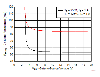
A common mistake is assuming as long as VGS≥ VGS(th), the FET is on and operates as intended in the application. This is not always the case. To ensure RDS(on) meets the data sheet limits, VGS must always be greater than or equal to the minimum value where RDS(on) is specified in the data sheet. This is often overlooked and can cause unexpected problems in the application. A customer using the CSD18541F5 had to change the design because the application used VGS = 3.3V instead of VGS = 4.5V. As shown in Figure 4-1, operating the CSD18541F5 with VGS < 4.5V, the slope of the curve is almost vertical and small changes in VGS(th) can result in exponential changes in RDS(on).
 Figure 4-1 CSD18541F5 RDS(on)
vs. VGS