Gehäuseinformationen
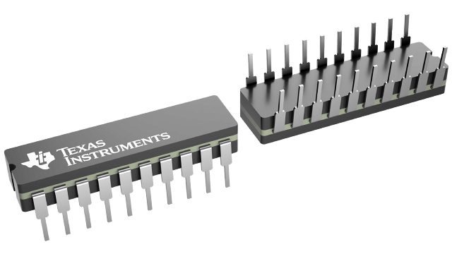
| Gehäuse | Pins CDIP (J) | 20 |
| Betriebstemperaturbereich (°C) -55 to 125 |
| Gehäusemenge | Träger 20 | TUBE |
Merkmale von SN54F541
- 3-State Outputs Drive Bus Lines or Buffer Memory Address Registers
- Data Flow-Through Pinout (All Inputs on Opposite Side From Outputs)
- Package Options Include Plastic Small-Outline Packages, Ceramic Chip Carriers, and Plastic and Ceramic DIPs
Beschreibung von SN54F541
The ´F541 octal buffer/line driver is ideal for driving bus lines or buffering memory address registers. The device features inputs and outputs on opposite sides of the package to facilitate printed-circuit-board layout.
The 3-state control gate is a 2-input AND gate with active-low
inputs so that if either output enable (![]() or
or ![]() ) input is high, all eight outputs
are in the high-impedance state.
) input is high, all eight outputs
are in the high-impedance state.
The SN54F541 is characterized for operation over the full military temperature range of -55°C to 125°C. The SN74F251 is characterized for operation from 0°C to 70°C.