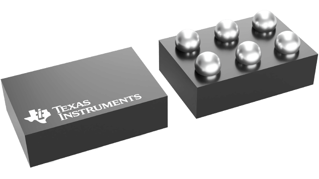
Gehäuseinformationen
| Gehäuse | Pins DSBGA (YFP) | 6 |
| Betriebstemperaturbereich (°C) -40 to 85 |
| Gehäusemenge | Träger 3.000 | LARGE T&R |
Merkmale von SN74AUP2G17
- Available in the Texas Instruments NanoStar&trade Package
- Low Static-Power Consumption
(ICC = 0.9 µA Maximum) - Low Dynamic-Power Consumption
(Cpd = 4.3 pF Typical at 3.3 V) - Low Input Capacitance (Ci = 1.5 pF Typical)
- Low Noise – Overshoot and Undershoot
<10% of VCC - Ioff Supports Partial-Power-Down Mode Operation
- Wide Operating VCC Range of 0.8 V to 3.6 V
- Optimized for 3.3-V Operation
- 3.6-V I/O Tolerant to Support Mixed-Mode Signal Operation
- tpd = 5.1 ns Maximum at 3.3 V
- Suitable for Point-to-Point Applications
- Latch-Up Performance Exceeds 100 mA Per JESD 78, Class II
- ESD Performance Tested Per JESD 22
- 2000-V Human-Body Model
(A114-B, Class II) - 1000-V Charged-Device Model (C101)
- 2000-V Human-Body Model
NanoStar is a trademark of Texas Instruments
Beschreibung von SN74AUP2G17
The AUP family is TI’s premier solution to the industry’s low-power needs in battery-powered portable applications. This family ensures a very low static- and dynamic-power consumption across the entire VCC range of 0.8 V to 3.6 V, resulting in increased battery life (see Figure 1). This product also maintains excellent signal integrity (see the very low undershoot and overshoot characteristics shown in Figure 2).
The SN74AUP2G17 contains two buffers and performs the Boolean function Y = A. The device functions as two independent buffers, but because of Schmitt action, it may have different input threshold levels for positive-going (VT+) and negative-going (VT–) signals.
NanoStar™ package technology is a major breakthrough in IC packaging concepts, using the die as the package.
This device is fully specified for partial-power-down applications using Ioff. The Ioff circuitry disables the outputs, preventing damaging current backflow through the device when it is powered down.
